CS International champions the versatility of the nitrides
The portfolio of devices based on GaN continues to strengthen and expand, with recent key additions including polychromatic and nanowire microLEDs, VCSELs with improved efficiency, and GaN HEMTs for power electronics that are targeting new markets.
BY RICHARD STREVENSON, EDITOR, CS MAGAZINE
Throughout the life of this publication, we have been covering major developments in GaN devices. In our very first issue, out 30 years ago, the cover story had the tagline Blue and Green: Commercial applications of short-wavelength light-emitting diodes. Within a few months, these fledgling GaN LEDs had been joined by laser diodes, thanks to another triumph of Shuji Nakamura. And over the last three decades the GaN device portfolio has mushroomed, with the introduction of microLEDs, VCSELs, and power and RF devices.
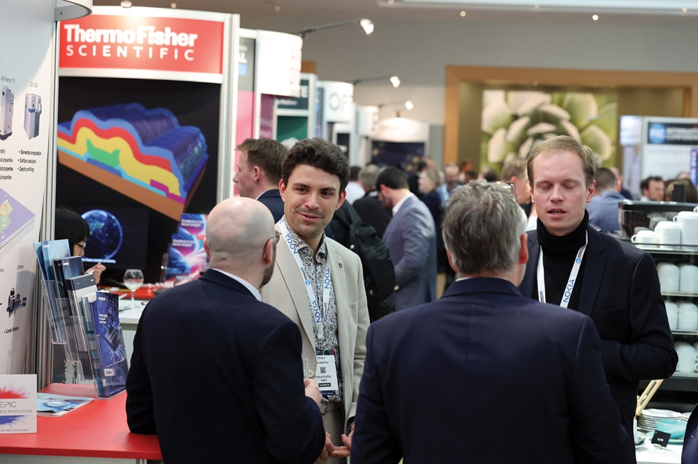
This year’s CS International, held in Brussels on the 8th and 9th of April, captured the breadth and progress of GaN, with presentations detailing advances on a number of fronts. Amongst these many talks, speakers from Q-Pixel, Porotech and Aledia described progress in microLED technology, which is promising to revolutionise displays; while advances in GaN-based VCSEL production were outlined by Tetsuya Takeuchi from Meijo University; and Roberto Crisafell from STMicroelectronics spoke about his company’s progress in GaN power devices.
Q-Pixel’s CEO Michelle Chen described the company’s polychromatic microLEDs that could simplify the production of AR displays.
Maintaining microLED momentum
It’s probably fair to say that the microLED is no longer a
new kid on the block. For a number of years there has been much interest in
commercialising this device for a wide variety of displays, from smartwatches
and VR/AR headsets to smartphones, automotive head-up displays and TVs. In many
of these applications, holding back commercialisation are challenges associated
with forming closely packed red, green and blue pixels with a sufficient yield,
precision and throughout to ensure acceptable production costs.
One promising solution to these challenges is the polychromatic pixel, a technology that’s been developed by both Q-Pixels and Porotech.
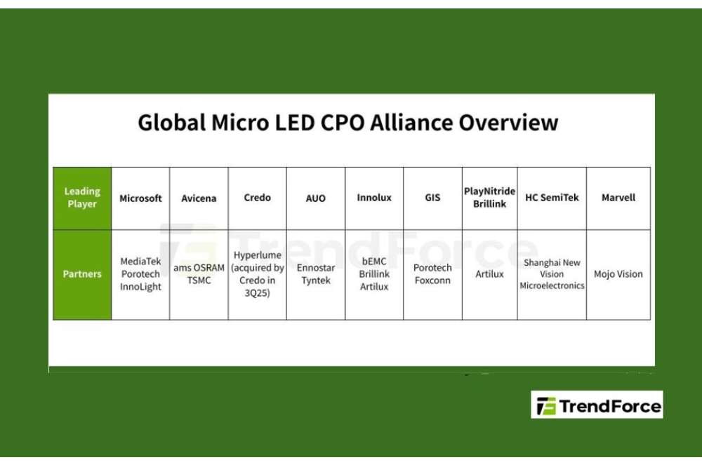
Porotech is working with many partners in Taiwan. Together,
they have created a supply chain for AR displays based on the microLED.
Speaking on behalf of Q-Pixel at CS International, company
CTO Michelle Chen remarked on the great opportunity provided by the display
industry, as well as the lack of progress in microLED technology. She put the
latter issue into perspective by pointing out that while the display industry
is worth around $168 billion, revenue for today’s microLED industry is
less than 0.5 percent of that figure.
It should be noted that the lack of success is not due to a lack of interest. “Major consumer electronics, including Apple, Meta, Samsung, LG, Sony and more, are all working on microLED technology,” explained Chen, who added that so far there’s little to show for this. Samsung has a microLED TV on the market, but it retails for $150,000, and despite much investment, Apple has not introduced a microLED smartwatch.
Money is going to keep flowing into microLED technology, says Chen, who reported that over $12 billion has already been invested in research and development, a figure forecast to climb to $35 billion by 2030. “The reason that industry keeps throwing money at this problem is that they see that the customer market is huge.”
Helping to drive all this investment is that, from a physics perspective, the microLED is an ideal source for displays. “As far as the physical advantages [of the microLED], there’s the brightness, lifetime, energy efficiency, and general robustness against ambient air,” championed Chen, who explained that the biggest challenge is the high-cost, due to complex assembly.
“This is really deeply rooted in the way full-colour displays have been made for a full colour range,” remarked Chen, who explained that this often involves red, green and blue subpixels from more than one material system, and the use of separate wafers for different colours prior to packaging.
Pierre Tchoulfian, Head of Technology and Device Engineering
at the Aledia, explained how the company’s nanowire technology addresses many
of the issues of conventional microLEDs.
Many developers of microLED technology are targeting the
AR/VR market. According to Chen, success in this sector demands a
very-high-resolution, needed to avoid what’s known as the ‘screen-door’ effect
– it’s the occurrence of thin, dark lines or a mesh, caused by gaps between the
pixels on a screen.
Having some success in this market is the Apple Vision Pro, which is based on microOLEDs. The resolution is high, reaching 3,400 pixels per inch, but the retail price is a concern – it’s over $3,000 – and power consumption is around 30 watts, met with a cumbersome battery pack that adds weight.
Chen argued that Q-Pixel’s technology is an attractive alternative to microOLEDs in this application. She explained that the company’s colour-tuneable polychromatic pixels can replace red, green and blue sub-pixels, leading to substantial cost savings.
“What we have is a single monolithic growth that is fully colour tuneable. It simplifies assembly a lot and it allows us to make very high-resolution displays,” explained Chen, who added: “The colour is tuned from red to blue by applying different electrical currents or voltages. This is a very industry compatible process. We don’t use any subpixels, there’s no regrowth, quantum dots, colour filters or polarisers.”
Setting many milestone over many years, Tetsuya Takeuchi’s
group from Meijo University are pioneers of the GaN-based VCSEL.
By adopting this approach, Q-Pixel is able to use standard
material, substrates and structures, as well as industry-standard tools that
are said to enable ease of integration and rapid, large-scale deployment.
Another strength of the company’s technology, according to Chen, is the small difference in voltage required to adjust the colour from red to blue. “This is very good from a systems perspective, because it’s more suitable for use with display drivers that are already on the market.”
Q-Pixel has already enjoyed notable success. “We have state-of-the-art red GaN brightness, and very low power consumption, less than 0.5 nanowatts per pixel when we’re operating in the green regime,” claimed Chen, who added that the company has produced prototype passive displays with up to 10,000 pixels-per-inch, and has the world-record for active displays, 6,800 pixels per inch.
Opportunities are also being explored for the company’s tuneable pixels in wearables in the health market, and also in automotive displays, where Chen claims microLEDs are a big contender. “Right now, current technologies simply don’t have the lifetime or robustness to last the lifetime of a car – but microLEDs can do that.”
At Meijo University, the most recent key breakthrough to
improving the performance of the GaN-based VCSEL has been the introduction of
in-situ cavity length control.
With a brightness that’s orders of magnitude higher than
what’s possible with OLEDs, Chen believes that microLEDs are also ‘perfect’ for
transparent displays that could be used outdoors.
“Again, the big bottleneck so far has not been the physics, it has been the cost,” says Chen. “How do we make these large-area displays at a reasonable price that people would want to spend money on?”
Q-Pixel has a solution, called Q-transfer, that is said to overcome the mass-transfer bottleneck. “This is our patented technology, enabled by the fact that we’re able to use this fully tuneable pixel. Not only is our resolution going to be higher, by virtue of the fact that we’re not dealing with sub-pixels, but because we’re only dealing with one kind of pixel, we can up the transfer speed and have higher throughput.”
One issue with all forms of display is that they require an incredibly high degree of perfection, because the human eye is so critical of dud pixels. While with some approaches, repair and replace is needed, that’s not the case with colour tuneable pixels. “If we have to adjust the wavelength, we can actually tune that electrically because we have this tuning capability.”
This feature may allow the microLED TV to become a reality for many. “Right now, you can buy a microLED TV, if you have $150,000 to spare, but we want to reduce that cost down by two orders of magnitude. And with our technology, we think it can be done,” argued Chen.
Porous polychromatic technology
Offering technologies that include one that’s a similar
approach to that of Q-Pixel, as well as the use of porous GaN material and
monochrome microLEDs, is the University of Cambridge spin-off Porotech.
Speaking on its behalf at CS International, VP Display & Head of
Taiwan, Kunal Kashyap, discussed the strengths of the company’s technology, and
its roadmap.
Established in 2020, Porotech has raised over $33 million, with Foxconn and GIS major shareholders. The company now has over 150 patents, spanning materials to optical modules; and employs more than 50 staff, located at either the UK headquarters and material lab, or at the R&D centre and production line in Taiwan.
Porotech has three core technologies. There’s porous GaN, allowing a tailoring of some critical properties of GaN; native monochrome single colours that span the entire visible range with the InGaN material system; and what’s referred to as Dynamic Pixel Tuning, which allows a microLED to emit any colour from the blue to the infrared.
Commenting on the latter, Kashyap remarked: “There are some trade-offs, which we are working on. But this is the holy grail technology.”
Initially, Porotech employed sapphire for the production of its microLEDs, but it has now switched to 8-inch silicon, as this is compatible with CMOS technology.
The company is working with a number of partners in Taiwan. Together they have created the world’s first hybrid bonding microLED ecosystem. EpiLEDs produces epitaxial wafers, pixelation is provided by PSMC, and Foxconn undertakes the hybrid bonding step. From here, Porotech’s product is sent on to Rayprus, to carry out back-end and flip-chip processes and produce a light engine. Completing the supply chain is GiS, offering waveguide and lamination services, and Foxconn subsidiary Jorjin Technologies, which is able to produce AR glass.
Working with these partners, Porotech is able to mass produce displays with pixels sizes of just 1.5 mm and 1.25 mm. These emitters are united with drive electronics using hybrid bonding, which is said to combine a high accuracy and a high yield with low die loss and high reliability. While pick-and-place and mass transfer has an accuracy of up to around 0.5 mm, according to Kashyap, with hybrid bonding an accuracy of 0.2 mm is the starting point.
The company’s first product, a microdisplay panel with a VGA platform and a pixel pitch of 3.75 mm, will enter high-volume production at the start of 2026. During summer 2026, this will be joined by Porotech’s second-generation technology, an SVGA format with a 2.5 mm pitch. And before the year is out, Gen 2+ will be in high-volume production, featuring resonant-cavity microLEDs. Providing collimated emission, this class of microLED improves coupling into the light engine, and enables a four-fold gain in efficiency at the system level.
Looking further ahead, Porotech plans to introduce its dynamic pixel tuning technology in 2027. This is already capable of spanning the visible spectrum, but prior to commercialisation, there needs to be an increase in brightness in the deep red.
An edge from nanowires?
Also competing for success in the microLED sector is French
chipmaker Aledia, which spun-out from CEA-Leti in 2012, and has spent the last
two years building a manufacturing line in Grenoble that houses €200 million of
production equipment. Today this pioneer of nanowire microLEDs employs 200
staff, with the majority in Grenoble and a handful in Shenzhen. Aledia has over
1,000 patents and more than 300 patent families, and it has raised more than
€500 million.
Speaking on behalf of the company at this year’s CS International, Head of Technology and Device Engineering Pierre Tchoulfian explained that Aledia is currently using 200 mm silicon as the foundation for its technology, with nanowires grown by MOCVD. However, scaling to 300 mm wafers is planned, with the company having demonstrated the capability to do so five years ago.
Throughout the remainder of this decade Aledia will be ramping its production capacity. In its 3,000 m2 cleanroom, it will be capable of running 100 wafers per week through its lines in 2027, increasing to 500 in 2030, with CMOS-like yields, says Tchoulfian. “But we have the room and the space to go to 3,000, if the market needs that.”
Tchoulfian touched on a number of issues that the emerging microLED industry is grappling with. They include: the reduction in the efficiency of this emitter with shrinking a microLED to a few microns in size; the lack of stability of red emission with current and temperature; mass transfer with a high yield and throughput; and the use of a flip-chip geometry that has two contacts on the same side of the device, when it’s preferable to have a top and a bottom contact.
Addressing many of these concerns is Aledia’s nanowire approach that produces blue microLEDs with an external quantum efficiency of 40 percent, for device sizes below 5 µm. Thanks to a favourable contact architecture, two microLEDs can be arranged in series and driven at 6 V or 9 V, enabling a 30 percent power saving at the panel level.
Drawing on a report from market analyst Yole, Tchoulfian claimed that by 2030 sales of AR headsets will total 25-30 million, with microLEDs accounting for around a 50 percent share. However, to enjoy that success, he argued that there’s a need to succeed on three fronts, related to power consumption, cost and brightness.
These requirements are inter-related. “You want the glasses to be 30 to 50 grams, and the display to be efficient,” said Tchoulfian, who pointed out that nanowires are a solution, benefitting from a photonic effect that enhances light extraction.
When it comes to cost, Tchoulfian believes that the full-colour displays for the glasses must be no more than $100. He sees epitaxy on 8-inch wafers and ultimately 12-inch wafers as the solution, with Aledia providing ‘mono-colour’ panels of red, green and blue, with the wavelength controlled by the degree of indium incorporation.
Improving the GaN VCSEL
Of all the mainstream light-emitting GaN-based devices, the
VCSEL is the least mature by a considerable margin. Its Achilles’ heel is its
mirrors. Unlike the GaAs VCSEL, where it’s relatively easy to produce a
distributed Bragg reflector from the pairing of GaAs and AlGaAs, a combination
with very similar lattice constants, there is no obvious nitride-based
combination for making the mirrors. Due to this, developers of this device
often turn to one or even two dielectric mirrors, and various approaches to
fine-tune the thickness of the cavity.
One promising option in the latter regard, detailed by Tetsuya Takeuchi from Meijo University, involves the introduction of in-situ cavity control.
Describing this refinement to delegates at CS International, Takeuchi claimed that in-situ cavity control is the third key advance in the GaN VCSEL fabrication process that has delivered a substantial increase in wall-plug efficiency, following in the footsteps of the development of a high-quality AlInN/GaN mirror and lateral confinement of the current and the optical modes.
Takeuchi explained that day-to-day variations in growth rate can be ± 2 percent, leading to unacceptable mirror losses. What’s needed is to ensure that this deviation is no more than 0.3 percent. “That’s why we installed the in-situ reflectivity spectrum measurement system from Laytec,” remarked Takeuchi.
With this tool, Takeuchi and co-workers collect wavelength spectral data, and a reflectivity intensity profile as a function of thickness. Drawing on all this information, the team has produced GaN VCSELs that benefit from very small deviations between the lasing wavelength and the centre wavelength for the distributed Bragg reflector. Lasers emitting at 420 nm produced 15 mW, and had a wall-plug efficiency of 21 percent. “I think this is still in the world’s highest number,” remarked Takeuchi.
Roberto Crisafulli, Director of the GaN and RF Business Unit
at STMicroelectronics, sees opportunities for this material in data centres,
motor drives and electric vehicles.
The rise of GaN power electronics
While GaN optoelectronics and RF electronics are
well-established markets that have existed for decades, significant sales of
GaN power electronics are relatively new. Power supplies for mobile devices
provided the first killer application, and now companies are looking to find new markets that will
benefit from the introduction of this wide bandgap semiconductor – it enables
higher efficiencies, far higher power densities, speedy switching, smaller
units and the absence of reverse losses.
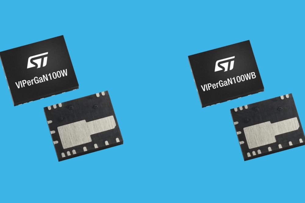
At CS International, Roberto Crisafulli, Director of the GaN and RF Business Unit at STMicroelectronics, spoke about two of the biggest opportunities for GaN that will help to increase annual revenue to around $2 billion by 2030: data centres and electric vehicles.
Crisafulli highlighted the importance of increasing energy efficiency in data centres, pointing out that this year their energy consumption is expected to total 250 TW-hours, and is tipped to double in the next few years.
“A key performance indicator is the so-called power-usage effectiveness, which is a metric to measure how much of the power fed to a data centre is really consumed by the IT infrastructure,” remarked Crisafulli. “Here we are still far from parity. The estimated average in 2025 is 1.3. It means that for every watt consumed to generate a digital response, there are still 300 milliwatts lost because of maintenance, because of cooling, because of auxiliary functions.” According to Crisafulli, these losses provide wideband materials in general, and GaN in particular, a great opportunity to help to achieve a target of parity.
He explained that data centres are undergoing tremendous change. The growth of AI is driving the replacement of uninterruptable power supplies with battery back-up units that will enable the integration of renewable energies into data centre power infrastructure. In addition, air-based cooling is being replaced with liquid-based variants.
Amongst these changes, power supply units are having to deliver far more power, due to the emergence of AI data and AI servers. Supplies of 1.2 kW and 1.5 kW are being replaced with more powerful variants, capable of delivering up to 12 kW.
“The total energy in the rack, which used to be in the range of 15 kilowatts, is now in reality already approaching 50 kilowatts, and this will rise and continue to rise up to 300 kilowatts until the end of the decade,” explained Crisafulli, who added that these higher powers are accompanied by a change in circuit topologies, and the way power is distributed in the system.
Crisafulli predicts that GaN will have a role to play here, enabling efficiencies to exceed 97 percent. Advances will also come from new circuit designs that incorporate this wide bandgap technology.
Within the electric vehicle market, Crisafulli sees an opportunity in the on-board charger, with GaN enabling the introduction of single-stage AC-to-DC converters that simplify the structure and trim costs. GaN may also win deployment in the traction inverter, and in local DC conversion.
GaN could also help to curb the global carbon dioxide footprint by improving the energy of motor drives. These drives, ignoring those associated with electric vehicles, account for about 30 percent of the world’s electrical energy consumption, and efficiencies are far from what’s possible.
There’s no doubt that the ST spokesman has an optimistic view for GaN, which he argues is on the verge of reaching more and more critical milestones in its adoption across various markets. “Partnerships to ramp-up production, to establish a resilient supply chain, is really key,” said Crisafulli, adding: “The achievement of cost and quality parity with silicon is really within reach.”
Thanks to progress of GaN on so many fronts, this material will surely be at the forefront of the CS industry for many years to come. And it will certainly take centre stage at the next CS International, to be held on 21-22 April, 2026.

