Researchers discover self-forming p-n junction
Scientists studying a promising quantum material called MnBi₆Te₁₀ have stumbled upon a surprise: within its crystal structure, the material naturally forms one of the world’s thinnest semiconductor junctions. The p-n junction is 3.3 nm thick.
They reported their work 'Spectroscopic evidence of intra-unit-cell charge redistribution in a charge-neutral magnetic topological insulator,' in the journal Nanoscale, in April 2025
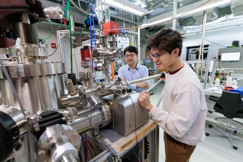
“This was a big surprise,” said Shuolong Yang, an assistant professor at the University of Chicago Pritzker School of Molecular Engineering (UChicago PME). “We weren’t trying to make this junction, but the material made one on its own, and it’s one of the thinnest we’ve ever seen.”
Researchers at the UChicago PME and Pennsylvania State University were studying the electronic properties of MnBi₆Te₁₀ by like letting electricity flow freely along its edges without any resistance.
While scientists hope that such materialslike MnBi₆Te₁₀ could someday be used in quantum computers or ultra-efficient electronic devices, but to work properly they need to have carefully balanced and distributed electrons. The team thought they had achieved the right balance by infusing MnBi₆Te₁₀ with antimony.
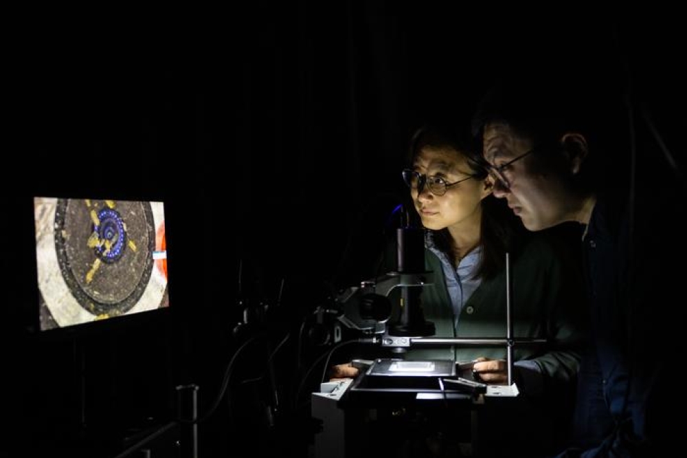
Regular electrical tests confirmed the material was, overall, neutral. When Yang’s team looked closer, using a technique called time- and angle-resolved photoemission spectroscopy (trARPES), they saw that within each repeating layer of the crystal, the electrons were not evenly spread. Instead, they were clumping up in some parts and leaving other parts with fewer electrons. This created tiny built-in electric fields within the material.
“In an ideal quantum material, you want a really uniform distribution of charges,” said UChicago PME graduate student Khanh Duy Nguyen, the first author of the new work. “Seeing this uneven distribution suggests that we may not enable quantum applications in the originally planned fashion, but reveals this other really useful phenomenon.”
These tiny regions acted like p-n junctions. But unlike manufactured p-n junctions, these ones form naturally as part of the crystal itself.
A boon for quantum and electronic applications
Because the new, naturally forming p-n junction is also highly responsive to light, it could be useful for next-generation electronics, including spintronics.
By modeling what was occurring within the crystal structure of MnBi₆Te₁₀, Nguyen, Yang and their colleagues were able to form a hypothesis about how it formed the p-n junctions. Introducing antimony into MnBi₆Te₁₀, they suspect, leads to swapping between manganese atoms and antimony, causing charge differences throughout the material.
While the finding adds complexity to efforts to use the material for certain types of quantum effects, it opens up new applications in electronics. It also paves the way toward further engineering of MnBi₆Te₁₀ so that it does maintain evenly distributed electrons—and can be useful in quantum engineering.
The UChicago PME team is finetuning ways of fabricating thin films of the material—rather than large, three-dimensional crystals. This could let them more precisely control the behaviour of electrons, either to boost quantum properties, or to boost the yield of tiny p-n junctions.
“This once again demonstrates the value of pursuing basic, fundamental scientific research and being open about where it leads,” said Yang. “We set out with one goal and found a surprise that led us in another, really exciting direction.”
Funding: This work was supported by the US Department of Energy (DE-SC0022960) and by the National Science Foundation through the Penn State 2D Crystal Consortium-Materials Innovation Platform (2DCC-MIP) under NSF Cooperative Agreement DMR 2039351.


