A symphony of semiconductors

Industry-facing academics championed the capabilities of devices
based on SiC, GaN and Ga2O3 at the recent European workshop on wide
bandgap power devices and applications.
BY RICHARD STEVENSON, EDITOR, CS MAGAZINE
It’s wonderful to listen to a beautiful voice singing a cappella, or a guitar in the hands of a maestro. But for many, this is eclipsed by great singer fronting a talented band or a professional orchestra playing a wonderful symphony. Why do we feel that way? It’s probably a reflection of the harmony, the interplay and the rich variety that comes from hearing different instruments playing different parts.
Parallels can be drawn between these musical experiences and the state of play in today’s power electronics industry. Once dominated by just silicon, this is now complemented by a growing portfolio of wider bandgap semiconductor, each with a particular set of attributes that come together to offer the designer a tremendous palette for constructing circuits. There’s GaN, delivering great efficiency and incredibly fast switching without a significant increase in cost while operating at several hundred volts; SiC, a more mature technology that’s well-suited to handling higher voltages; and Ga2O3, with the potential to outperform this duo, thanks to an even higher bandgap, along with the promise of lower costs that stem from melt-growth of crystal boules.
Promotion of this symphony of semiconductors came from many of the speakers at the IEEE Workshop on Wide Bandgap Power Devices and Applications (WiPDA) in Europe, held on 16-18 September, at the Royal Welsh College of Music & Drama, part of Cardiff University. At this venue, where delegates were treated to traditional Welsh music in the run up to the conference banquet, a number of keynote speakers emphasised the need to improve the efficiency in electrical systems, through refinement to circuit design and the introduction of better devices, as well as outlining the pros and cons of the many diodes and transistors within the wide bandgap portfolio.
Johan Kolar from ETH Zurich suggested that the power electronics
industry is in its fourth era, and championed a move to a circular
economy that involves recycling of materials when moving to the fifth
era.
The big picture
It’s easy to feel overwhelmed and powerless when thinking about climate change. This makes it tempting to bury of one’s head in the sand. But that’s never ideal, given that action is required – and particularly so for us, given that our industry has a very important role to play in decarbonisation.
A good reminder of the alarming consequences of global warming, along with the opportunities for power electronics to combat this, despite the implications on global resources resulting from a ramp in their production, came from the opening keynote address from Johann Kolar from ETH Zurich.
Kolar began his presentation by pointing out the need for a clean energy transition, which demands an all-electric society. He explained that today CO2 emissions stand at 40 gigatonnes, and questioned whether humanity is going to succeed in meeting the goal of net zero by 2050, suggesting it may take 50 years from now to reach this target.
If we are not going to reach net zero, it’s prudent to prepare for climate change, argued Kolar, who outlined efforts to accommodate a rise in sea level.
He explained that there are engineers in The Netherlands that are thinking about building really huge dams to enclose the North Sea and prevent roughly 25 million people from having to deal with increasing sea levels. By the end of this century, many people other parts of the world could also be having to deal with a rise in sea levels, including those in parts of east Asia, Brazil and the east coast of the US. “Time is running out,” warned Kolar.
The ETH academic went on to consider the energy requirements of humanity, which currently stand at around 2.5 kW per person. By 2050 this figure will have increased a little, while the global population will have climbed to 10 billion, leading to a total power demand of around 27 TW.
The good news is that this figure is dwarfed by the power from the sun. If we consider just the sunlight falling over land, its power is still roughly a thousand times higher than that required by humanity.
Helping us to tap into this power is the rising deployment of renewable energy. According to forecasts shared by Kolar, deployment of photovoltaics and off-shore wind power are set to increase at compound annual growth rates of 9 percent and 7 percent, respectively, until 2050. By then sunlight will provide 8.5 TW of power generation, and off-shore wind another 5 TW.
For these renewable deployments, power electronics has a fundamental role to play, argued Kolar, who pointed out that it is needed to convert the electricity generated by these sources into a form that can be fed into the grid. However, he believes that improvements are needed to these critical components, such as reductions in cost, failure rate, weight and losses, as well as an acceleration in the time-to-market.
During his presentation, Kolar provided a whistle-stop tour of the evolution of the modern power electronics industry. He sees the starting point as 1958, the commercial introduction of the thyristor. This device dominated through to the 1970s, before the introduction of the first MOSFETs, the first bipolar transistors and then IGBTs, along with new circuit topologies and some microelectronics. The next big breakthrough came in 1995, with the introduction of superjunction technology. By the turn of the millennium digital power had also attracted much attention.
Over the last decade and more, SiC has been an increasingly significant player in the power electronics sector, added Kolar: “In industry, from 2015 you could see more and more applications of silicon carbide components. This, for sure, is one of the X technologies. What is an X technology? It is aiming for a factor of ten improvement.”
SiC and GaN both offer this, with substantial reductions in on-resistance over silicon. However, more thought needs to be given to making the most of this with appropriate circuit design. While engineers have been designing circuits for many years, Kolar emphasised that there is still much room for improvement in their architectures, and offered a number of examples where his team have made significant advances.
Moving towards an all-electric society will help with decarbonisation, but there is a price to pay, a significant consumption of resources. Due to this, Kolar is championing the need for far greater re-use of electronic materials. He argued that if we move to 25 TW of installed electrical energy generation, due to four steps associated with conversion from source to load, total global installation would equate to 100 TW. He went on to point out that 20 years of lifetime means that there would be 5 TW of electronic waste per year. This means that we need to not just think of the technology and the design. Kolar is urging a shift from a linear economy, which is already generating close to 50 million tonnes of waste per year, to a circular one that involves the re-use of critical materials, and zero end-of-life waste.
Device comparisons
A more detailed look at the family of power devices came from Florin Udrea, a Cambridge University academic and the founder and Chief Technology Officer of Cambridge GaN Devices.
Udrea pointed out that all the wide bandgap materials outperform silicon in one key characteristic: the breakdown field strength. “Silicon carbide is ten times better, GaN even more, and arguably diamond and gallium oxide are the star contributors there – they are classified as ultra-wide-bandgap semiconductors.”
While the breakdown field is the most important metric for power semiconductors, there are others that are also important, according to Udrea, such as thermal conductivity. Judge on this front, silicon is reasonable, but SiC and diamond are much better. “This is where gallium oxide has a problem, because it has very low thermal conductivity. It behaves more like an oxide than a silicon carbide,” remarked Udrea.
Another metric that matters is carrier mobility. “Gallium nitride is incredibly interesting, because it’s the only material that beats silicon not only in terms of the critical electric field being higher, but also in terms of the mobility,” remarked Udrea. He pointed out that the carrier mobility in Ga2O3 is relatively low, and while silicon has a high intrinsic mobility, it collapses after doping and falls at elevated temperatures.
Udrea summarised the properties of all the key materials in a table (see Table 1). He championed those with a wider bandgap, reasoning that this leads to a higher critical electric field that in turn enables the fabrication of scaled-down devices that feature a smaller drift region with a higher doping concentration, key to ensuring a higher efficiency.
Table 1. The strengths and weaknesses of the key materials in power
electronics, according to Florin Udrea. Green denotes strength, yellow a
satisfactory performance, and red highlights weakness.
Of the leading alternatives to silicon, while those with the ultra-wide bandgaps may have the biggest promise, Udrea is sceptical about their prospects. Although he believes that diamond and Ga2O3 are interesting from a materials science perspective, he is concerned by the low thermal conductivity and an absence of p-type doping in Ga2O3, and the absence of n-type doping in diamond.
Although the coming years will see a substantial rise in the sales of wide bandgap devices – led by SiC MOSFETs, SiC Schottky barrier diodes, and GaN HEMTs – Udrea is adamant that silicon will still have a significant role to play. That’s partly due to its strengths, in terms of its reliability, ease of manufacturing, infrastructure, cost, as well as its diversity, attributes that provide a significant advantage, according to Udera.
What’s more, silicon is not as far behind its wider bandgap rivals as one might expect, in terms of performance. With a critical field that’s lower by a factor of around ten, and an on-resistance proportional to the cube of this, one might expect silicon devices to be completely outclassed by the likes of GaN and SiC. But that’s not the case, with silicon overcoming its limit described by Baliga’s figure of merit, due to a number of sophisticated device designs, such as the superjunction and the power MOSFET.
Udrea highlighted the revolutionary performance of the silicon superjunction transistor: “It’s not 10 percent or 20 percent better than the MOSFET. It’s orders of magnitude better.” This is realised by increasing the doping in the drift region by a factor of around 100.
Another important silicon device is the IGBT. This has evolved over several decades, with the latest design, known as a trench field stop IGBT with an electron injector, combining strengths of punch-through and non-punch-through structures by incorporating a very thin drift region and an electron-injection mechanism.
The superior material properties of SiC and GaN allow for far better performance when replicating designs based on silicon. Udrea illustrated this, comparing the silicon power MOSFET with that made from SiC. Thanks to a ten-fold hike in the critical electric field, it’s possible to shrink the thickness of the doping region by this factor – and by also increasing the doping concentration in this region by around 100 times, there’s the potential for a 1000-fold hike in conductivity. In practice, such gains are not possible, due to a relatively high channel resistance and a low mobility, but despite this, the gains are substantial.
“But remember, we are not competing against this now,” warned Udrea, who explained that when up against superjunction devices, SiC is only better by a factor of seven or eight – and when it comes to the IBGT, it’s even less.
Opportunities for SiC and GaN
However, there are other advantages with SiC, such as its capability to switch at higher frequencies. To make the most of these strengths, one needs to fully understanding the properties of this material, argued Udrea. He cited a study by Kimoto Tsunenobu’s group from Kyoto University that uncovered that compared to the A-face of SiC, the C-face has a higher mobility and a higher critical field strength.
The SiC devices on the market today are predominantly offering blocking voltages between around 600 V and a few kilovolts. However, there’s a peak in performance at around 1 kV, according to Udrea.
He shared data showing contributions to the specific on-resistance from the channel, the drift region, the substrate and other factors, for SiC MOSFETs operating at 600 V, 1.2 kV and 3.3 kV. At the highest voltage, drift resistance dominates, and at the lowest resistance the channel resistance is the most significant factor. At the 1.2 kV sweet spot, where there are substantial sales for the traction inverter, both the channel and the drift are important. Looking to the future, Udrea wants to see SiC superjunction devices for high voltages, finFETs for lower voltages, and finFET superjunctions for devices handling around 1 kV.
In silicon the finFET is well established, with Udrea describing this class of transistor as the most advanced digital structure of today. He championed the development of SiC devices based on this architecture, using the SiC MOSFET as a starting point. For this device, with a p-body width of more than 1 µm, the pair of depletion charges and channel charges are balanced by the gate charge (see Figure 1). Shrinking the width of the p-body causes depletion charges to merge and then disappear, and re-position all the gate charge in the channel. When the p-body is reduced to 30 nm or so, quantum effects also aid performance, which benefits from total inversion in the bulk rather than on the surface.
According to Udrea, SiC finFETs with these dimensions benefit from an increased electron charge, along with bulk inversion and elimination of the transverse electric field, two factors that reduce the likelihood of Coulombic scattering. All these gains help to trim the on-resistance.
Working with partners at Mirise Technology Corporation, an R&D institution supported by Denso and Toyota, Udrea and colleagues at Cambridge University have produced a range of finFETs with different fin widths. With fins just 35 nm wide, mobility increases to more than 200 cm2 V-1 s-1, a substantial increase over the standard mobility in SiC transistors.
Udrea also outlined progress in superjunction devices made from SiC, which unlike some other wide and ultra-wide bandgap semiconductors, can be doped n-type and p-type, a requirement for this device architecture. He predicts that this device will be commercially available within a few years, and based on modelling, explained that performance can be maximised by optimising both the width and doping of the pillars, and moving from a 2D to a 3D superjunction.
…and GaN
Udrea went on to champion GaN, comparing the silicon laterally-diffused MOSFET to the GaN HEMT. Thanks to internal piezolelectric fields in the latter, no doping is needed to produce a channel that provides a carrier mobility of around 2000 cm2 V-1 s-1. Additional strengths are: a high critical electric field strength, enabling a ten-fold reduction in device size; and an opportunity for isolation on the chip, enabling the construction of power IC blocks.
According to Urea, makers of GaN devices fall into two camps. There are those that make discrete enhancement-mode HEMTs, including Cambridge GaN Devices, Innoscience, and Infineon; and there are those that employ a cascode structure and use a depletion-mode HEMT, an option pursued by Transphorm and Nexperia. Udrea pointed out that the latter approach has the benefit of addressing the poor gate reliability of the GaN HEMT, but with two devices in series, there are reverse recovery losses.
Another key differentiator in the market is the level of integration. While the discrete is the norm, some companies have gone further. One example is Navitas, which has integrated the driver. “This solution has worked, and it’s in the market, and has done very well in the low power [regime],” remarked Urea, but he feels that at higher powers there are concerns related to heat generation and efficiency.
At Cambridge GaN Devices they have adopted a different approach, referred to as sensing and protection. “We chose to integrate what is necessary, but we left the driver outside,” explained Udrea. Merits of this design include a high degree of robustness, and the opportunity for the engineer to access the driver. This allows the use of very intelligent, multi-channel drivers, a level of functionality that is much easier to realise in silicon than GaN.
Like SiC, which is advancing with superjunctions and finFETs, the architectures for GaN are advancing. Udrea highlighted the multi-channel E-mode HEMT that his team has helped to pioneer, an innovation led by Yuhao Zhang’s group at Virginia Polytechnic Institute and State University. This device, operating in a cascode configuration, is said to benefit from extremely good conduction, thanks to the introduction of five layers of two-dimensional electron gas. And in terms of the combination of breakdown voltage and on-resistance, it is breaking new ground, according to Udrea.
Figure 1. One option for lowering the on-resistance of SiC transistors is to switch from a MOSFET to a finFET.
Enhancing production processes
Supporting the UK’s capabilities in producing compound semiconductor devices is the recently constructed Centre for Integrative Semiconductors at the University of Swansea. Its strengths were described by Mike Jennings, Head of Energy and Power Engineering at Swansea University, who explained: “Our interest is working with industry, to take prototype devices and scale them with our manufacturing process. We are working across all materials.”
Drawing on investment from the UK government from 2019 to 2024, and supported by industrial partners, the Centre for Integrative Semiconductors has around 1,000 m2 of cleanroom, equipped with more than 60 tools that can process 150 mm and 200 mm wafers. Within this facility, focused on power electronics, is an industrial process line for the design, fabrication, testing and pilot production of SiC, and a tool for the growth of Ga2O3. The centre is also home to advanced dielectric and dry etch specialities. “Dry etch is probably our forte,” claimed Jennings. “We can etch pretty much any material to any depth, through our close relationship with KLA.”
Mike Jennings, Head of Energy and Power Engineering at Swansea
University, is helping to lead efforts at the recently established
Centre for Integrative Semiconductors.
Jennings discussed a range of materials and devices, including opportunities related to the 3C form of SiC. While this has a lower bandgap than GaN and the 4H polytype of SiC, and thus a lower critical electric field strength and breakdown voltage, it is a very attractive candidate for making robust devices. “If you want a really reliable MOS interface gate oxides, then cubic silicon carbide is the dream,” enthused Jennings, who explained that 3C-SiC has a bigger band offset with SiO2 than silicon. Due to this, Fowler-Nordheim tunnelling across the oxide-semiconductor barrier, the main failure mechanism, is 1.5 times less in 3C-SiC than silicon, and around 2.25 times less than it is for 4H-SiC. In addition, there is the promise of a far lower density of interface states in 3C-SiC than 4H-SiC.
Experimental work by Jennings and colleagues is underscoring the potential of 3C-SiC. Capacitance-voltage measurements on the interface between the semiconductor and the dielectric formed with a range of treatments has revealed a density of interface states below that of silicon, and far, far lower than that for 4H-SiC.
Jennings said that the most exciting work that he’s currently engaged with is that of the vertical GaN transistor. He compared this device with the lateral GaN HEMT, which benefits from a high mobility in the two-dimensional electron gas that gives some great characteristics, such as the absence of reverse recovery losses and extremely fast switching. “But the blocking voltage depends on the distance between the drain and the gate, which is problematic when commercialising technologies above 650 volts, such as a large-area die,” remarked Jennings, who also pointed out the lack of avalanche capability.
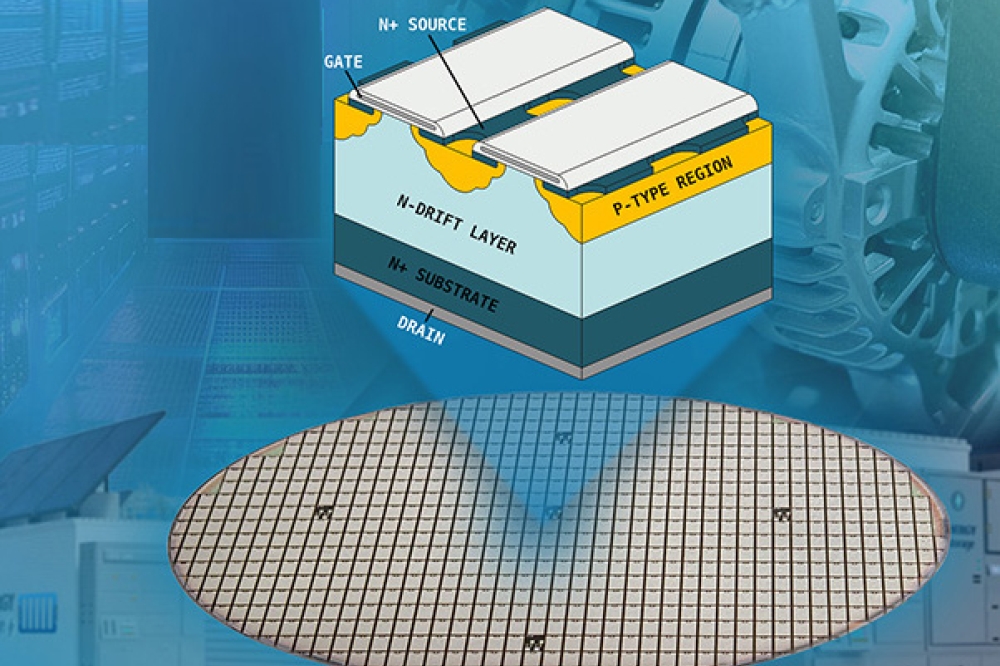
Figure 2. Strengths of the vertical trench GaN MOSFET include a blocking
voltage that is governed by vertical dimensions and the possibility for
avalanche capability.
A vertical trench GaN MOSFET (see Figure 2) addresses both these issues, and features a standard MOS gate that is easy to drive. However, there are concerns associated with the mobility in the channel and the need for p-type doping.
“The question is: Can this be competitive? Can we get that channel mobility good enough that it will be commercially viable?” remarked Jennings, who also pointed out the need to extract the heat from this high-current device. To help to answer these questions, Jennings and colleagues fabricated quasi-vertical GaN-on-SiC MOSFETs with a 2.5 µm-thick drift layer that are designed to handle up to 200 V. Initial results are encouraging, with a very low series resistance of 8.5 mΩ cm2, and a breakdown voltage of 220 V.
Florin Udrea, an academic at the University of Cambridge and the CTO of
Cambridge GaN Devices, championed advances in SiC and GaN devices, such
as superjunctions, fins and multiple channels.
Opportunities with Ga2O3
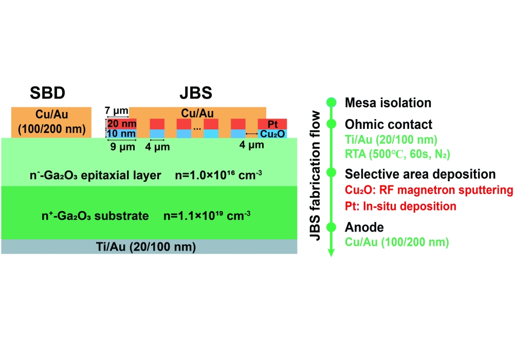
A keynote presentation from Martin Kuball from the University of Bristol detailed the promise of Ga2O3, alongside approaches to accommodate its weaknesses, by pairing this oxide with other materials.
In terms of substrate size, it’s already possible to buy 4-inch material, and there are research demonstrations up to 6-inch, according to Kuball: “You could think about commercialisation at that moment in time, because the substrate size of gallium oxide is already at the level where you could do manufacturing.”
Kuball pointed out that devices made from Ga2O3 have the potential to withstand very high electric fields while exhibiting an incredibly low on-resistance. However, there’s a need for thermal management, to compensate for the low thermal conductivity of this oxide, and to introduce new materials to provide p-doping within the device, if it’s required.
Among a number of devices that Kuball and his colleagues are developing, arguably the most exciting is that incorporating a superjunction, based on the pairing of n-type Ga2O3 and p-type diamond, which is used to fill trenches. Back in 2021 the team simulated such structures, using realistic properties for diamond that account for a lower thermal conductivity due to the grain structure, and found that this still led to a dramatic improvement in thermal management. This work also showed that by optimising charge balancing and adjusting the field distribution, it’s possible to boost the breakdown voltage quite significantly.
Martin Kuball, Director of the UKRI Innovation and Research Centre
REWIRE at the University of Bristol, is driving development of Ga2O3
devices featuring hetero-integration.
Working with Stanford, Kuball and coworkers have started working towards the fabrication of superjunction devices, looking at sidewall properties. Initial structures have a breakdown voltage of 900 V, limited by the peak electric field not sitting at the interface between the two materials. Addressing this could increase the breakdown to 5 kV or more.
“Just to point out, it’s not good diamond. It’s nanocrystalline diamond, so there’s still need for optimisation,” revealed Kuball, who views these early results as quite promising.
He clearly has many plans for the future, as do all of those working on the development of wide bandgap devices and the design of the circuits that incorporate them. There is much to look forward to, due to these harmonious efforts.
Around 130 delegates attended the IEEE Workshop on Wide Bandgap Power Devices and Applications in Europe, held in mid-September at Cardiff University.


