
Scientists break GaN HEMT limits using novel gate dielectric
Scientists from the universities of California Berkeley and Stanford have broken a long-standing performance barrier in GaN HEMTs.
By integrating a ferroic gate dielectric that leverages negative capacitance, they simultaneously enhanced ON current and reduced gate leakage; two metrics traditionally at odds with conventional dielectrics governed by classical electrostatics.
GaN HEMTs are key components in 5G, radar, and space communications, but they face fundamental trade-offs. Maximising gate control to achieve high ON current often requires a Schottky gate, which suffers from high gate leakage. Conversely, reducing leakage by adding conventional dielectric weakens the gate’s electrostatic coupling to the channel, thereby limiting drive current and overall performance.
By integrating a negative capacitance dielectric, the researchers have removed this constraint. They say their results demonstrate that negative capacitance can break conventional electrostatic limits in a broad class of transistors that rely on quantum well, 2DEG channels such as those based on III-V compound semiconductors.
Furthermore, from an applied standpoint, they think their approach could redefine the design of next-generation high-frequency GaN devices, as well as emerging wide and ultrawide bandgap materials for high-power RF electronics.
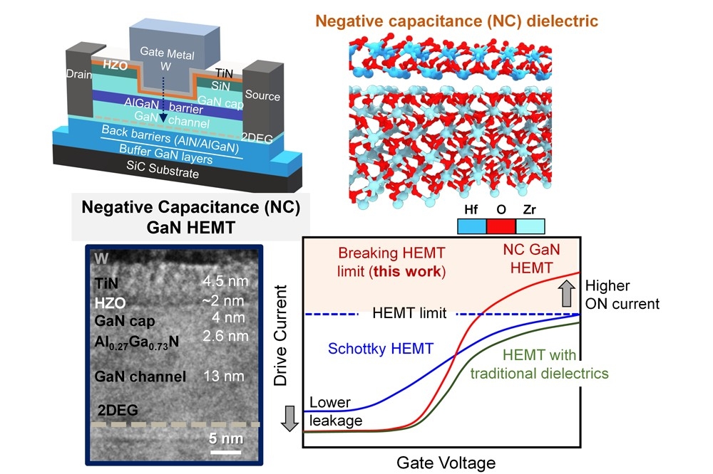
The team fabricated two types of HEMTs on the same N-polar AlGaN/GaN heterostructure: (1) a baseline Schottky HEMT with metal gate directly on the GaN cap layer, and (2) a negative capacitance HEMT with a ~2 nm HZO dielectric stack between the GaN cap and gate metal.
High-resolution transmission electron microscope imaging confirmed the mixed ferroelectric and antiferroelectric phases responsible for negative capacitance. Electrical measurements revealed a ~30 percent higher gate capacitance in the NC-HEMT compared to the Schottky control, along with a ~3× increase in ON current and over an order-of-magnitude reduction in gate leakage.
Importantly, the negative capacitance GaN HEMT devices exhibited nearly hysteresis-free transfer characteristics, indicating a cleaner dielectric/GaN interface and stable operation.
The capacitance boost using HZO stack was originally tailored for silicon devices in Sayeef Salahuddin’s lab at UC Berkeley EECS. Drawing inspiration from prior work, the team—led by Asir Khan and Urmita Sikder from the Salahuddin group—has now successfully integrated negative capacitance gate dielectric technology into GaN.
Jeong-Kyu Kim, co-lead author and a graduate student in Srabanti Chowdhury’s group at Stanford, noted that customising the gate stack specifically for ultra-scaled GaN transistors could unlock even greater gains in frequency, efficiency, and output power for future telecommunications systems.
Reference
A. I. Khan et al., 'Negative capacitance overcomes Schottky-gate limits in GaN high-electron-mobility transistors'; Science (2025)


