

Evaluating radiation hardness with UV laser pulses
By delivering radiation-induced damage with a high spatial resolution, UV pulsed laser irradiation technology is providing a powerful approach for assessing GaN power electronics in space applications.
BY FENG ZHOU, MAI ZHANG, CAN ZOU AND HAI LU FROM NANJING UNIVERSITY
Within the palette of compound semiconductors, GaN has emerged as a promising candidate for next-generation aerospace electronics, due to its superior material properties. Of those, arguably the most important is the high displacement threshold energy, which effectively suppresses irradiation displacement damage.
However, GaN-based power devices do have their weaknesses, suffering from pronounced susceptibility to single-event effects, induced by high-energy heavy ions that are prevalent in space. When these ions bombard semiconductor devices, high linear-energy transfer occurs, leading to single-event burnout that’s triggered by ionisation effects and charge accumulation. This chain of events is a major issue, threatening to result in severe performance degradation and even catastrophic device failure.
Due to these severe concerns, it is critical to enhance the irradiation hardness of GaN power devices to single-event burnout. Unfortunately, that’s not a straightforward task, as irradiation experiments primarily rely on heavy-ion accelerators, which suffer from prolonged experimental cycles, exorbitant costs, and inherent limitations in achieving precisely localised irradiation and dynamic in-situ testing. Consequently, it is imperative to develop a cost-effective test system with a high spatial resolution that’s capable of supporting both static and dynamic irradiation experiments.

Table 1: Summary of pulse laser irradiation experimental system. SPA,
TPA and 3PA are short for single-photon, two-photon and three-photon
absorption, respectively.
The good news is that pulsed laser irradiation produces similar conditions to heavy-ion irradiation. The latter induces single-event effects via particle-scattering-generated electron-hole pairs, while pulsed laser irradiation generates electron-hole pairs through the photoelectric effect. Note that pulsed laser irradiation offers a number of distinct advantages over heavy-ion irradiation, including precise spatial control of the incident position, extended operational duration, superior experimental reproducibility, and cost-effectiveness. Thanks to these merits, pulsed laser irradiation is a viable method for simulating single-event effects induced by heavy ions, and enables the establishment of correlations between heavy ions and the pulsed source. With pulsed laser irradiation, the two main physical mechanisms used to simulate single-event effects are single-photon absorption and two-photon absorption.
One photon or two?
For irradiation investigations using single-photon absorption, one must employ a laser with an energy higher than the bandgap of the device. As each absorbed photon generates an electron-hole pair, the pulsed laser source can induce carrier generation in a micron-scale area of the device under test. Thanks to these conditions, researchers can realise a high accuracy and a high test-efficiency, enabling high matching with heavy ion irradiation.
A key difference with two-photon absorption is that as the laser energy is beneath the material bandgap, almost no carriers are generated at low light intensity. Switching to a high light intensity addresses this issue, so long as the light is strongly focused, enabling two-photon absorption in the material that leads to the generation of electron-hole pairs (the principle of three-photon absorption or four-photon absorption is similar to two-photon absorption). Note that efforts based on the absorption of multiple photons are better suited to devices covered with thick metals, or those requiring the optical source to be directed to the backside.

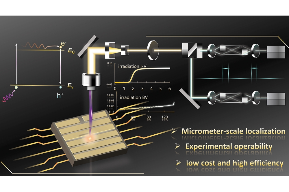
Figure 1. The UV pulsed laser simulated irradiation testing system comprises the following integrated modules: (1), a UV pulsed laser source module with a repetition rate of around 10 kHz that generates 266 nm UV pulses that are shorter than a nanosecond and a maximum single-pulse energy at the surface of the device under test (DUT) of more than 15 nJ; (2), an optical coupling module that efficiently couples and delivers the laser output to the surface of the DUT; (3), a two-dimensional scanning displacement platform, providing a scanning range of 3 cm by 3 cm with sub-micron resolved irradiation for localised sensitivity mapping of devices; (4), a variable-temperature-control module, offering precise temperature regulation across 80-420 K with a stability of ±0.1 °C, facilitating temperature-dependent irradiation effect studies; and (5), a real-time electrical characterisation module, enabling in-situ electrical measurements during irradiation, to capture dynamic responses of the DUT. (b) Equivalence between pulsed laser and heavy ion (linear energy transfer, LET, as a function of the effective laser energy, Eeff). This plot has been obtained using: an experimental impact ionisation energy for GaN of 8.9 eV; a density for GaN of 6.1 g cm-3; a lasing wavelength of 266 nm; and a single-photon absorption coefficient at that wavelength of 1×105 cm-1. As the lasing energy is 4.66 eV, well above the GaN bandgap of 3.39 eV, single-photon absorption occurs in the active region and the two-photon absorption coefficient can be considered as zero.
Today, experiments involving the pulsed laser irradiation of GaN power devices are concentrated in institutions such as the French National Center for Scientific Research, the University of Bordeaux, the US Naval Research Laboratory and the National Space Science Center of China (NSSC) (see Table 1 for a summary of the relevant laser system parameters). Among these efforts, only the NRL has reported studies on UV pulsed laser irradiation targeting wide-bandgap GaN based on single-photon absorption. Furthermore, no studies have been published on dynamic electrical characterisation under pulsed laser irradiation.
Addressing this omission is our research team from Nanjing University. We have independently developed an advanced UV pulsed laser simulated irradiation testing system (for details, see Figure 1 (a)).
Using this pulsed laser system, we have investigated a number of matters. They include: the equivalence between a pulsed laser and heavy ions; single-event transient, and single-event burnout; irradiation-sensitive area mapping; dynamic double-pulse switching; un-clamped inductive switching robustness; and power-conversion efficiency. All these studies promote the application of pulsed laser experimental technology in GaN power devices.

Figure 2. (a) SET test circuit (model: PSPL5580, bandwidth: 15 GHz) and (b) corresponding waveforms. (c) Irradiation-induced photocurrent mapping image.
Before determining pulsed laser experimental conditions and optimising functionality, we considered the equivalence between pulsed lasers and heavy ions. The absorption of a 266 nm pulsed laser in GaN can be calculated from the laser intensity in the semiconductor, the free-carrier absorption cross section, the free-carrier density, and single-photon and two-photon absorption coefficients. We have also calculated the effective laser energy, using values of 0.144 for the passivation layer reflectivity, 0.22 for the reflectivity of the interface between the passivation layer and the barrier layer, and 0.212 for the reflectivity of the interface between the barrier layer and the buffer layer. Combining these equations with others that consider how the effective laser energy varies with distance, and the change in electric field intensity with distance, provides us with an equation for determining the equivalent linear energy transfer value for a pulsed laser (see Figure 1 (b)).
Under pulsed laser irradiation, single-event transients resulting from single-photon absorption can lead to disturbances in the current signal that influence the device’s high-frequency operation and its stability. We are able to investigate this with our single-event transient test circuit (see Figure 2 (a)), featuring three high-frequency bias tees.

Figure 3. Pulse laser irradiation system and dynamic switching circuit.
Double-pulse switching waveforms for (b) p-GaN and (c) MIS HEMTs, and
reverse recovery waveforms for GaN diodes.
The gate, source and drain terminals of the device under test are connected to the common ports of the three bias tees. Subsequently, the AC ports of the bias tees are interfaced with three channels of an oscilloscope to capture single-event transient waveforms. To ensure precise focusing on the sample surface and laser incident positioning, we use a CCD camera. An adjustable power supply provides power to the laser system. Once the laser is turned on, we use an optical attenuator to adjust the effective incident energy of the pulsed laser.
Extracted single-event transient waveforms are shown in Figure 2 (b). They show that gate and drain currents of the GaN HEMT increase, indicating that there is a dissipation passage between the gate and drain for the irradiation-induced carriers. We are able to investigate this in more detail with our pulsed laser experimental techniques, which offer an advantage over approaches based on heavy ion irradiation – for that case, it’s challenging to observe single-event transients, due to the randomness of particle incidence and large-area irradiation.
To determine the single-event burnout for devices, we apply a bias voltage to the device under test through a high-voltage source under pulsed laser irradiation. This experimental arrangement is simpler than that for single-event transients, which use a similar setup to that involving heavy ion irradiation. During the test, the single-event burnout depends on the bias voltage, as well as the pulsed laser equivalent of heavy ions. It is worth noting that since the pulsed laser provides micro-area localised irradiation, the device’s susceptibility to irradiation may be weaker than that of heavy ions, and a higher bias voltage is desired to obtain critical single-event burnout.

Figure 4. (a) Un-clamped inductive switching circuit setup in a UV pulse
laser irradiation experimental system. (b) Critical un-clamped
inductive switching and failure waveforms.
Irradiation-sensitive area mapping
Within our pulsed laser irradiation system is a fluorescence spectroscopy module, which can perform mapping scans according to different bias voltages during irradiation. Drawing on this feature, we are able to observe the local current size on the device and thus identify its sensitive areas.
To gain this insight, we use the 2612B source meter (programmable by software) to provide the bias voltage. We apply an output voltage of up to 400 V and have a pulse current capacity of 10 A.
One strength of our system is that it has a measurement accuracy at the picoamp level. However, to optimise this accuracy, it is critical to select a suitable measurement range, based on the photocurrent size of the device. After scanning, our system automatically performs data storage and graph drawing.
Illustrating the capability of our instrumentation is Figure 2 (c). This photocurrent map reveals that the sensitive areas of the GaN HEMT (highlighted in the red stripe area) have a wider distribution than adjacent areas under pulsed laser irradiation, confirming that they are susceptible to local charge deposition and are irradiation-sensitive areas.
Integrating a double-pulse switching circuit into our pulsed laser irradiation system allows us to evaluate the dynamic characteristics of GaN power devices. Based on equivalence evaluation, we have used an effective laser energy of 0.432 pJ to emulate a linear energy transfer value that’s equivalent to 82.7 MeV cm² mg-1 in heavy-ion experiments (see Figure 3 (a)).
We have obtained plots of dynamic switching waveforms (400 V/10 A) of p-GaN HEMT and GaN MIS-HEMT devices, along with reverse recovery waveforms of the GaN rectifier (see Figures 3 (b) - (d)). Data shows that devices exhibit nanosecond-scale fast switching performance under UV pulsed laser irradiation.
Assessing robustness
Robustness of non-avalanche p-GaN gate HEMTs against dynamic overvoltage and transient surge-energy shocks is critical for device applications, especially for extreme irradiation switching applications. While un-clamped inductive switching characteristics of p-GaN HEMTs are partially understood in terrestrial application scenarios, their behaviour under extreme irradiation conditions remains unexplored.
We are lifting the veil on this with a UV pulsed laser irradiation system that’s integrated with an un-clamped inductive switching module (see Figure 4 (a) for an illustration of this system, and that of the 650 V p-type GaN HEMT under test).
With this experiment, during irradiation the device is initially turned on to charge the load inductor. Then the HEMT is turned off, forcing the energy stored in the inductor to surge toward the device under test. During this process, we use an oscilloscope to record real-time waveforms for the un-clamped inductive switching voltage and current. Laser irradiation is realised by using wire bonding to mount the HEMTs onto a custom-printed circuit daughterboard.
Under irradiation, we find that the critical dynamic overvoltage of the device is approximately 897 V, beyond which catastrophic failure occurs (see Figure 4 (b)). In contrast, without irradiation this metric reaches 1109 V. Based on these two values, we have determined that the dynamic overvoltage capability of the irradiated device deteriorates, with a degradation rate of 19 percent.
To determine energy loss, we integrate power over time during the charging and discharging phases associated with un-clamped inductive switching. This reveals that the irradiated device exhibits a consistently lower energy loss than its unirradiated counterpart across the entire range of surge currents.
These experiments uncover a concurrent reduction in dynamic overvoltage and energy loss. The fall in dynamic overvoltage signifies a decline in device endurance, while the diminished energy loss implies a decreased sensitivity to charge imbalance, governed by un-clamped inductive switching. We attribute these characteristics to the pre-filling of acceptor traps within the GaN buffer layer, with electron charges generated by single-event irradiation. To further enhance dynamic overvoltage hardness, it is crucial to alleviate the drain-side strong electric-field caused by irradiation. These findings and hardening guidelines offer critical insights to improving the robustness of p-GaN HEMTs in irradiation applications.

Figure 5. (a) Cross-sectional scanning tunnelling electron microscopy image of an irradiation-hardened epitaxial structure. (b) 3D schematic of an irradiation-hardened GaN-on-SiC HEMT. (c) Power factor correction circuit, and system efficiency versus output power for an irradiation-hardened p-GaN HEMT and a 400-V irradiation-hardened silicon VDMOS (JHCS6N40NJR).
Power conversion efficiencies
We have also employed our pulsed laser technology to scrutinise the power-conversion efficiency of irradiation-hardened devices. They feature additional epitaxial material and a device structure that forms hole accumulation and dissipation passages. The robust design includes an additional 8-nm thick Al0.1Ga0.9N layer to effectively confine the charges in a narrow heterojunction interlayer region (see Figure 5 (a)), and a source-connected partitioned gate structure design to quickly discharge the radiation-induced charges to the outside of the device (see Figure 5 (b)).
Measurements of these irradiation-hardened p-GaN HEMTs operating at 500 W at 300 K under a linear energy transfer of 82.7 in a continuous-conduction power factor correction circuit have a power-conversion efficiency of 96 percent. That’s far higher than a power-conversion efficiency of 400 V for irradiation-hardened silicon VDMOS – it’s just 91 percent.
Our wide range of investigations using pulses of UV for irradiation showcase the strength and breadth of this technique, which will help to assess, enhance and demonstrate the capabilities of GaN HEMTs for deployment in space.


