
SNU team outlines roadmap for 2D 'gate stack'
A research team from Seoul National University (SNU) has outlined a roadmap for ‘gate stack’ engineering, a core technology for two-dimensional transistors. The study was published in the journal Nature Electronics on September 11 2025.
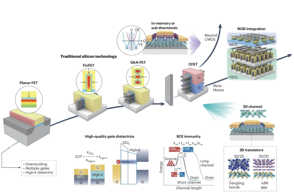
CMOS technology has driven improvements in performance and integration density for decades. However, further scaling is increasingly constrained by physical and electrostatic limits. 2D semiconductors are attracting growing attention as the 'beyond-silicon' approach.
Chip firms and research institutes, including Samsung, TSMC, Intel, and Imec, have already incorporated plans to adopt 2D semiconductor transistors as next-generation technology into their roadmaps after the mid-2030s.
With substantial R&D programs already underway, 2D semiconductors are shifting from a long-term prospect to a rapidly emerging next-generation core technology. This is not an easy transition, with ‘gate stack’ integration technology being a significant obstacle to commercialising 2D semiconductors.
As the structure that electrostatically controls channel conduction, Gate stack quality determines the device performance and stability.
However, directly applying existing silicon transistor processes to 2D semiconductors not only degrades the quality of the dielectric but also causes issues like defects at the interface and leakage current.
Developing new materials and process integrations tailored to 2D interfaces is considered the most critical task for commercialising 2D semiconductors.
In this recent paper, a research team led by Chul-Ho Lee from SNU's College of Engineering department of electrical and computer engineering, has analysed various gate stack integration methods and quantitatively benchmarked them against performance metrics, to help outline future technological development directions.
First, the research categorises gate stack integration approaches into five categories: (1) van der Waals (vdW) dielectrics, (2) vdW-oxidised dielectrics, (3) quasi-vdW dielectrics, (4) vdW-seeded dielectrics, and (5) non-vdW-seeded dielectrics.
Each method was evaluated against metrics such as interface trap density, equivalent oxide thickness, gate leakage density, threshold voltage, and supply voltage. The team benchmarked these metrics against the goals outlined in the International Roadmap for Devices and Systems (IRDS). This process yielded a systematic development roadmap that serves as a reference for both academia and industry.
The research team also demonstrated the potential for gate stacks incorporating ferroelectric materials to be scaled up into next-generation devices. For instance, utilising ferroelectric-embedded gate stacks enables the realisation of ultra-low-power logic, non-volatile memory, and in-memory computing.
Furthermore, the researchers specifically outlined practical requirements, including Back-End-of-Line (BEOL) compatibility, low-temperature deposition (< 400°C), wafer-scale uniformity, and long-term reliability. This emphasises real-world industrial applicability beyond theoretical discussion.
This research confirmed the feasibility of ultra-low-power, high-performance transistors but also proposed specific technical directions considering future monolithic 3D integration and BEOL-compatible processes.
Furthermore, the technologies presented in this study are expected to become core foundational technologies driving the advancement of next-generation ICT infrastructure, such as AI semiconductors, ultra-low-power mobile chips, and ultra-high-density servers.
Lee stated, “The biggest obstacle to commercialising 2D transistors is the implementation of high-quality gate stacks. This research presents a standard blueprint to overcome this challenge, making it highly impactful both academically and industrially. We plan to actively expand research on device-level integration and commercialisation through industry-academia collaboration.”


