The vertical GaN transistor: Time for take-off
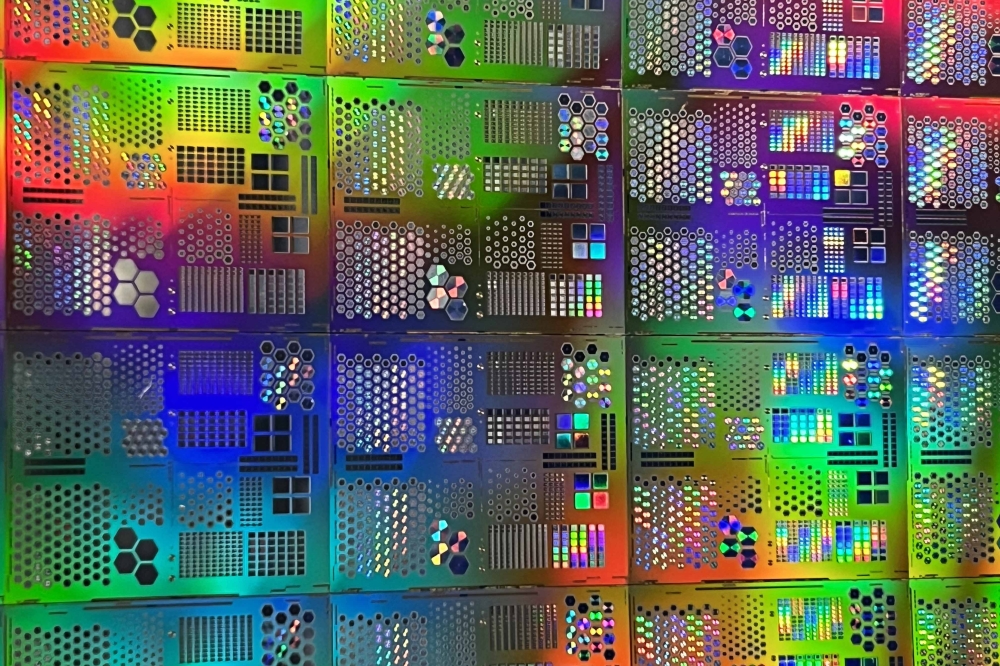
Using 200 mm foundries, MIT start-up Vertical Semiconductor will produce finFETs on engineered substrates.
BY RICHARD STEVENSON, EDITOR, CS MAGAZINE
There’s a lot to be said for the vertical GaN transistor. Compared to its horizontal sibling, it delivers a higher breakdown voltage and current for a given footprint, while offering superior reliability, and simplifying thermal management.
However, efforts by start-ups to commercialise the vertical GaN transistor have flopped, and today it is the lateral variant that enjoys commercial success, thanks in part to establishing a ‘killer’ application, the fast-charging of mobile devices.
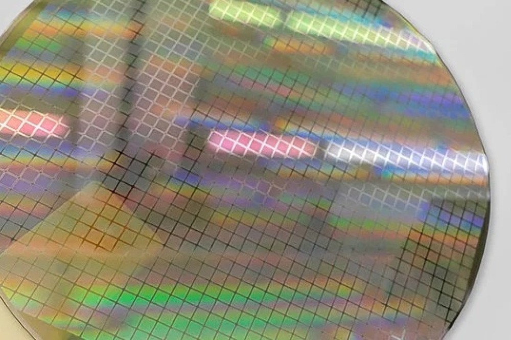
Holding back the success of the superior geometry is its native foundation. As well as a high price tag, the GaN substrate is limited in size, with a typical diameter of just 50 mm. This prevents device fabrication on established 200 mm lines that benefit from economies of scale, as well as the use of more modern processing equipment.
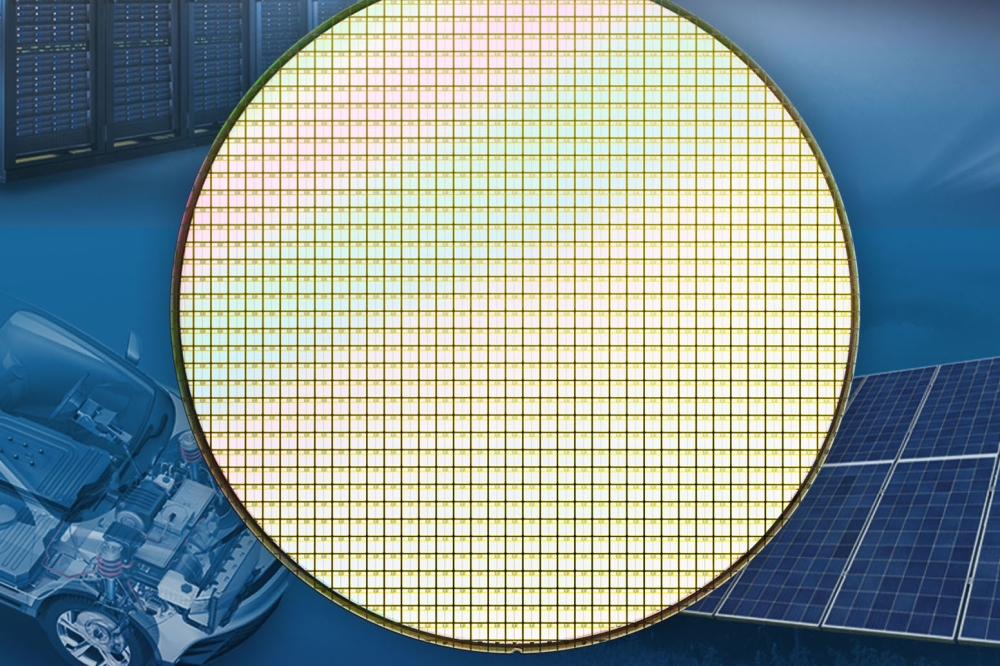
Trailblazing a solution to these limitations is Vertical Semiconductor, a spin-out of Tomás Palacios’ group at MIT. Vertical is pioneering the use of 200 mm engineered substrates for the manufacture of GaN finFETs, an approach that allows the outsourcing of chip production to numerous foundries with silicon CMOS capabilities.
Founded last year, Vertical initially maintained a low profile, before announcing this October that it’s secured $11 million in funding. This investment will be used to develop commercial devices on foundry lines that will enable the start-up to target the data-centre market. Here there is a much-publicised ramp in energy demand, due to the growth of AI, and GaN finFETs promise to make an impact by trimming energy losses and simplifying infrastructure. According to Vertical, its devices can increase efficiency by up to 30 percent, and enable a 50 percent reduction in the footprint of the power supplies.
It should be noted that the finFET is not the only class of vertical GaN transistor. For well over a decade, the global GaN research community has been exploring different designs, including the current-aperture vertical electron transistor and the trench MOSFET. A significant weakness of both those designs is the demand for either epitaxial regrowth or the inclusion of p-type GaN layers – requirements that lead to a hike in fabrication complexity and cost, or an inferior channel carrier mobility.
Vertical is pursuing a different design, the finFET. This class of transistor only requires n-type GaN layers, so it can be produced without epitaxial regrowth.
Another strength of the finFET is the much-coveted normally-off operation, resulting from narrow fin channels that ensure all electrons are depleted at zero bias.
Back in 2019, benchmarking of the 1.2 kV GaN-on-GaN finFETs produced in Palacios’ group, using a figure-of-merit for power switching that included all possible conduction and switching losses, highlighted the superiority of this design over all state-of-the-art silicon and SiC power transistors and large-area GaN R&D devices.
This success has provided the core technology for Vertical, co-founded by Palacios and the company’s CEO and CTO, Cynthia Liao and Joshua Perozek.
The backstory
While Perozek’s path to CTO is a familiar one, involving the progression from a researcher in Palacios’ group to technical lead in the start-up, Liao has arrived from a markedly different background.
After completing a degree in business administration at Western University, Ontario, she spent the first ten years of her career working in energy infrastructure, as well as energy and climate policy.
“I came to MIT as a mid-career MBA student in the Sloan-Fellow programme. And my goal was to actually pivot my experiences into a more entrepreneurial journey, and specifically using technology that I felt was quite exciting at MIT to make an impact around climate and energy.”
Through a class at MIT, Liao met Perozek and Palacios. Enthused by the technology and its potential, she started supporting this lab, talking to potential customers. And after the class ended, the collaboration continued with much success, including the winning of competitions, the securing of initial support, and entry into an accelerator programme.
When Liao and Perozek graduated in the summer of 2024 they decided to incorporate the company.
Over the last year or so, Vertical has secured capital that will support its efforts to develop its first prototype packages, slated for sampling by the end of this year, before progressing to the launch of what’s described as a fully integrated solution. To execute these plans, Vertical will be working with suppliers of engineered substrates, and providers of epiwafer and foundry services.
Helping to bridge the transition between R&D and volume production is the work Perozek undertook during his time in Palacois’ group, involving transfer of the technology from the research lab to the MIT Lincoln Laboratory. These efforts led to the fabrication of the first GaN finFETs on 200 mm wafers.
Another goal that Liao and her colleagues have been focusing on is generating demand with customers.
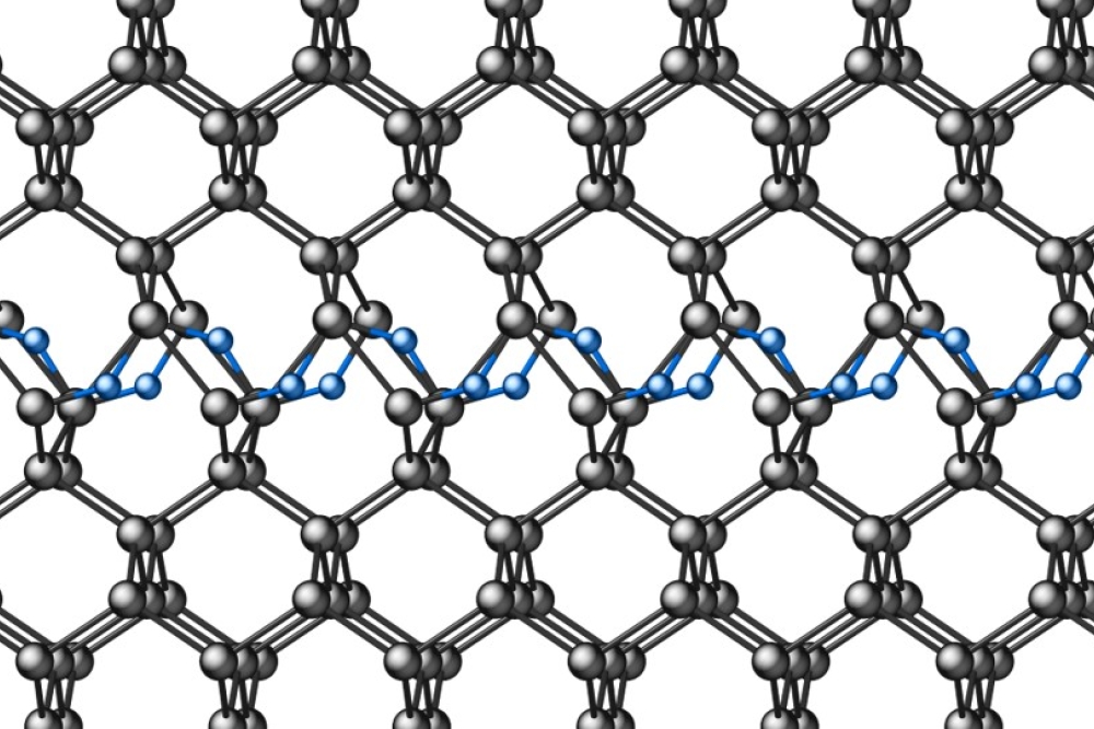
Vertical’s GaN finFETs feature a bottom contact on the backside of a 200 mm engineered substrate.
Targeting data centres
“We are engaging across the data centre power value chain, and working with customers to understand how that architecture is continuing to evolve, in order to serve the demands of these XPUs going into the future,” says Liao.
Data centres have various requirements for power, ranging from lower-voltage point-of-load to solid-state transformers and solid-state circuit breakers.
“We're excited about plugging ourselves into these different application areas, which go into industrial power supplies, grid interfaces, and renewable energy technologies,” remarks Liao.
She also sees opportunities for the team’s finFETs in electric vehicles, where they promise to extend the driving range while offering a smaller form factor than the incumbents. But there is a downside of this market from Vertical’s perspective: the is the relatively long qualification times, which hamper the start-up from establishing itself in the power market.
“Our goal is to get these devices into customers' hands, and then work on the reliability and qualification needed for automotive production,” explains Liao, before adding that despite this priority, Vertical has started to engage with customers in the mobility and vehicle space.
The team at Vertical, now totalling six employees and expected to increase in number over the coming months, is developing a portfolio of devices with blocking voltages from 100 V to 1,200 V.
These GaN finFETs will be shipped as packaged die. “If people want bare die, we’re happy to provide that. But we find that packaged is preferred,” says Liao.
Over time, Vertical will expand its range, introducing devices with higher blocking voltages. That’s relatively easy to do, as thanks to growth on engineered substrates, the thicker GaN layers needed to withstand higher voltages do not introduce significant bow and warp.
But for the next 12 months, Vertical’s focus will be on producing working devices at scale with a foundry partner, and creating a clear path towards qualification. “That's our number one target,” says Liao.


