When every microsecond counts

Infineon’s CoolSiC JFET is a new class of switching device that enables power distribution systems to be immune from delays.
BY ROBERT ROESNER AND BARIS YILDIRIM FROM INFINEON TECHNOLOGIES
Once an electrical circuit is overloaded, you would expect a circuit breaker to respond immediately and reliably. But in today’s fast-moving, electrified systems, such as electric trucks, AI data centres and modern industrial manufacturing plants, ‘immediately’ is no longer fast enough. In these scenarios every microsecond counts, and standard protective devices, such as fuses, relays, and moulded case circuit breakers, are failing to keep up within the rapidly growing world of AC and DC power systems. Those components were designed for a different era, when millisecond response times were fast enough. But they lack the speed, precision, and intelligence demanded by today’s systems, shortfalls that have serious consequences.
Take a modern electric truck, for example: if a fault occurs during high-speed charging or rapid acceleration, and the device isn’t disconnected quickly, critical components can overheat, threatening to damage power electronics and even cause a fire. Similarly, in an AI data centre, if a short circuit occurs on a power bus and isn’t quickly isolated, an entire rack can be crippled, resulting in data loss, downtime and expensive hardware damage.
Figure 1. The discrete CoolSiC JFET family has been developed with solid-state power distribution applications in mind.
Both these examples illustrate how vulnerable modern systems are to electrical faults, especially now that vehicles, factories, and data infrastructures are increasingly electrified, compact, and complex. This changing landscape places new demands on power distribution systems: higher voltages, faster protection, and significantly tighter safety margins.
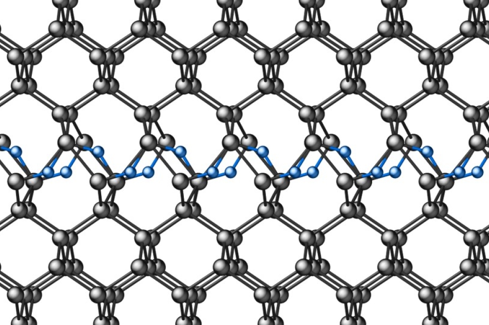
Figure 2. Volume conduction and vertical current flow enable low resistance and efficient high-voltage switching.
Alternatives with flaws
Solid-state protection devices based on the MOSFET are already commercially available. They address many shortcomings of mechanical switches – including contact wear, slow reaction times, and imprecise thresholds – but they have their limits, especially in high-voltage or high-current applications.
While SiC MOSFETs outperform their silicon-based cousins by offering better overall switching performance, plus a higher efficiency and improved thermal characteristics, even this class of transistor cannot fully close the gap when it comes to robustness under fault conditions or sustained operation in linear mode. One significant downside of the SiC MOSFET is its relatively high on-resistance (RDS(ON)), leading to the need for larger devices that drive up both cost and complexity. To manage the resulting thermal load or enable higher current levels, designers have to resort to parallelizing multiple devices, an approach that demands deep product and system expertise.
Furthermore, SiC MOSFETs have limitations in avalanche robustness and linear-mode stability, constraining the fault-handling capabilities of these devices under extreme conditions, like pre-charging or un-clamped inductive switching. These limitations force engineers to compromise, rather than deploying an optimal solution – trading speed for safety, or efficiency for design simplicity. But in modern systems where fault isolation has to happen as fast and reliably as possible, these trade-offs aren’t just inconvenient, they’re potential points of failure.
For next-generation applications, such as solid-state circuit breakers, battery disconnect switches, and hot-swap electronic fuses in AI data centres, system designers need something more: a technology that combines an ultra-low RDS(ON) with thermal stability in linear mode and robust avalanche behaviour to ensure fast, safe and reliable performance under harsh conditions.
Figure 3. In normally-on JFETs, current flows through the volume (or bulk) channel with minimal resistance.
Built to protect
To overcome the limitations of mechanical protection devices and extend the capabilities of solid-state switches, our company, Infineon Technologies, has developed a new type of discrete switching device: the CoolSiC JFET (see Figure 1). Based on a JFET cell design, our device takes a different approach to high-voltage switching in power distribution. It is designed specifically for modern applications, where milliseconds are too long and conventional MOSFETs are falling short. Rather than building on conventional MOSFET architectures, this device is engineered for efficiency, ruggedness, and simplifying system design in demanding environments.
The CoolSiC JFET is based on a purely vertical trench structure (see Figure 2) that minimises conduction losses and maintains a stable electrical performance, even under changing load conditions. This form of transistor addresses significant weaknesses associated with MOSFET-based solutions, which often require larger cooling elements or derating to stay within safe limits.
In contrast, the CoolSiC JFET retains its efficiency across a wide load range, including continuous line operation, a condition that occurs in electric vehicle battery disconnects and server power distribution.
One reason for the consistent efficiency stems from how the SiC JFET conducts current. Unlike the SiC MOSFET, which relies on a thin surface-level n-channel, current flows through the entire volume of the semiconductor. Due to bulk conduction, JFETs are normally on, resulting in reduced channel resistance (see Figure 3). While the drift region – which blocks voltage – limits both device types similarly, JFETs benefit from lower resistance in the channel itself. Thanks to this, SiC JFETs have a lower overall RDS(ON) for the same chip size, enabling systems to run cooler. This translates into better efficiency in high-voltage designs.
Another attribute of the SiC JFET is its avalanche ruggedness. In fault scenarios such as short circuits and overloads, this device responds quickly and consistently, handling sudden voltage spikes and current surges. This fast reaction helps prevent equipment failure, and mitigates risk at the system level. In addition, the JFET can absorb high energy internally, eliminating the need for elaborate external clamping circuits and simplifying the overall protection scheme. The upshot: a more compact, cost-effective, robust design.
Figure 4. In the cascode configuration, a MOSFET is added so that the JFET behaves like a normally-off device.
Though naturally a normally-on device, the JFET can behave like a normally-off switch when it’s combined with a low-voltage silicon MOSFET in a cascode configuration (see Figure 4). In this configuration, the pairing provides the benefits of JFET conduction and ruggedness, alongside the control characteristics of MOSFETs. Merits of the MOSFET-JFET combination include reliable and predictable switching behaviour, as well as essential features for applications like solid-state breakers or industrial protection switches. And another strength enjoyed by designers is the flexibility to implement the JFET-MOSFET into existing control architectures with minimal changes.
Note that other arrangements also yieldimpressive results. For example, a pair of JFETs is an attractive option in systems requiring bidirectional current flow, such as battery disconnect switches or AC protection devices. In this case, two JFETs in a source-to-source configuration offer directionality, while increasing design flexibility and facilitating integration into complex architectures.
Equally important is the device’s packaging. Housing die in a Q-DPAK surface-mount package with top-side cooling allows for efficient heat extraction away from the chip (see Figure 5). It’s an arrangement that simplifies heat management and helps realise a higher power density, particularly valued in applications where space and cooling capabilities are limited. Helping to excel in these regards is our .XT interconnect technology – it provides additional support associated with transient thermal performance, and helps to handle demanding load cycling, ensuring long-term reliability, even in harsh environments.
It would be wrong to view CoolSiC JFETs as simply drop-in replacements for MOSFET-based devices. They also offer design-level benefits for building more compact, more reliable protection with fewer external components and reduced system complexity. Whether in battery disconnect switches for electric vehicles, electronic fuses in AI servers, or fast-acting solid-state circuit breakers in industrial environments, the ability to respond quickly and reliably can make all the difference.
What engineers need to know
While CoolSiC JFETs offer many benefits for modern power distribution design, they don’t behave exactly like conventional MOSFETs. In order to get the most out of them, engineers need to take a few key design aspects into account early in the process.
As these devices are often used in safety-critical systems, like electric vehicles or industrial power supplies, it is crucial to understand how they behave under fault conditions. For example, if the gate signal fails or a short circuit occurs, the system must remain safe. It is important to consider known safety standards at an early stage, including those from the International Electrotechnical Commission and Underwriters Laboratories.
However, one of the most significant points is the control of the device. When a JFET is used in a cascode configuration, it’s crucial to carefully control the gate signals. Doing so prevents unwanted switching operations, especially during rapid voltage changes or when switching on. Other important goals for a designer are a good layout and a reliable clamping circuit to ensure safe and consistent operation of the switch.
It’s also essential to avoid overlooking thermal design and mechanical details. Long-term reliability may be influenced by factors such as the PCB layout, the connection to cooling elements, and the way in which the device tolerates vibrations or temperature changes over time.
Thanks to top-side cooling, JFETs can dissipate heat more effectively than conventionalpackages, thereby simplifying thermal management – but only if the component is properly connected to a heat sink or copper area on the board. Design engineers need to note that early consideration of heat flow helps avoid issues later on. And these engineers should also be aware that testing and validation under real-world conditions is an absolute must in systems where safety is a top priority.
In short, the CoolSiC JFET offers a powerful combination of system simplicity, efficiency, and reliability, especially in designs where space is at a premium and response times critical. However, thoughtful integration is essential for unlocking new levels of performance in next-generation power systems. This advice applies to electric vehicles and AI data centres, and also to microgrids and renewable energy systems.
Figure 5. The top-side cooled package simplifies cooling management.
Keeping pace with tomorrow’s systems
Some of the key trends in power supply systems are that they are becoming faster, more compact and increasingly software-defined. As a result, mechanical protection methods struggle to keep up. That’s a disaster in today’s highly electrified world, where every microsecond counts and reliability, speed, and safety are more important than ever. These needs are behind the launch of the CoolSiC JFET – a high-voltage switch that offer engineers new tools to meet modern system demands, while responding to faults instantly and reliably.
Whether protecting AI servers, disconnecting EV batteries, or enabling semiconductor-based power switches in industrial systems, JFETs help to build safer, smarter, and more easily scalable power supply architectures. By reducing system complexity and improving thermal performance, they also allow for more compact designs without sacrificing robustness.
Plans are now in place to expand the portfolio with additional package and module options, covering a broader range of applications and current ratings. For engineers developing next-generation electrified systems, this expanding family of devices offers an opportunity to rethink protection methods at the speed demanded by modern systems, and to make power distribution ready for what’s next.


