
Rare earths ready for GaN power electronics
As power electronics players turn to GaN-on-silicon epiwafers to manufacture high performance devices, Translucent has unveiled a stress-free alternative. Compound Semiconductor reports.
Will industry embrace Translucent's novel templates for III-N MOCVD?
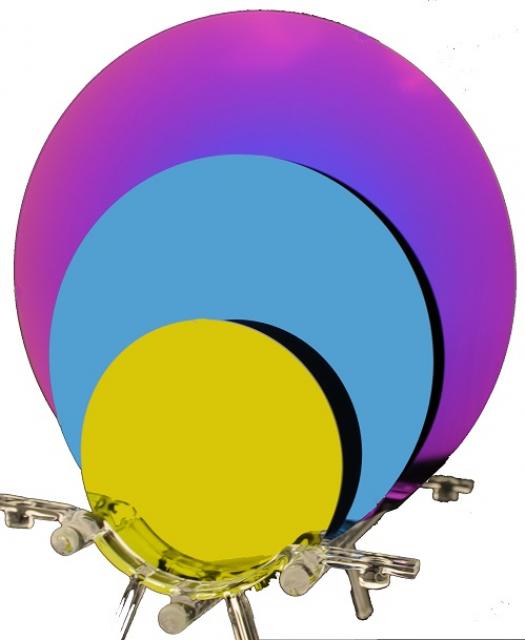
Earlier this year, up and coming developer of templates for III-V and III-N epitaxy, Translucent, unveiled 300 mm silicon templates with a rare earth oxide buffer layer.
Unique in the growing world of GaN-on-silicon, the US-based company hopes manufacturers of power devices, keen to embrace the technology without the stress of lattice mismatches, will adopt the template.
"GaN-on-silicon has matured and many companies now consider it to be an established technology, but we looked at it and asked, is the current method the best that can be used?" says Andrew Clark, vice president of engineering at Translucent.
"We've been working with rare earth oxides for many years now, and realised that a new buffer material between the GaN and silicon would help," he adds.
As Clark explains, the insulating buffer layer of crystalline rare earth oxide (REO) - typically erbium oxide - is lattice matched with the silicon on its lower surface.
As a result, the upper surface can be engineered so defect growth during GaN epitaxy is more akin to GaN-on-sapphire than GaN-on-silicon, reducing wafer curvature and bowing. This also spells good news for manufacturers looking for an easy transition from GaN-on-sapphire to GaN-on-silicon.
The REO layer is also an insulator, and as such, will increase a transistor's breakdown voltage while blocking the interactions between the silicon substrate and III-nitride layers that kill device performance.
Consequently, Clark reckons the buffer layer could trim GaN thicknesses by at least 25% and even remove the need for the AlN interlayers commonly used to minimise silicon-GaN interactions.
And of course, this reduces III-V materials and epitaxy process costs while offsetting the additional cost of the rare earth oxide layer.
"When you use an AlN buffer... you also have to clean the MOCVD chamber and platen inbetween runs," highlights Clark. "But we will supply the rare earth oxide on silicon as the starting wafer, so we're reducing the cycle times for MOCVD processes."
"Rare earth materials are now a relatively cheap materials to buy, and having done cost analyses at volume, [a manufacturer] is going to save dollars on cycle times," he adds.
Industry adoption
But benefits aside, will device manufacturers bite? After all, Translucent is introducing what is fundamentally a new GaN-on-silicon epitaxy concept. Clark remains confident.
For starters, the technology comes relatively free of the GaN-on-silicon IP infringement issues that plague industry newcomers.
"This is clean IP," says Clark. "If you are a new company looking to get into GaN-on-silicon, do you take a risk and copy [existing fabrication methods] or do you invest in new IP and build your product on this?"
Importantly, the company has also worked with development partners to produce a solid process. Strong materials data has been well received by a number of companies and European consortia working on GaN-on-silicon, especially those focusing on 200 mm wafers.
"The infrastructure for [GaN-on-silicon] technology is established and many in the industry believe the next two years will be a critical phase in which the market should grow and stabilise," he says.
"Importantly for us, these companies are now returning to development cycles and looking to improve performances with a better process," he adds.
What's more, demonstrating that their REO buffer layer can stretch to 300 mm without succumbing to the dreaded wafer bow bodes well for manufacturers looking to fabricate the devices of the future.
With the key driver behind the move from native wafers to silicon substrates being to use depreciated 200 mm CMOS fabs and slash manufacturing costs, Clark and colleagues realised that they had to develop templates of this size from word go.
But as the vice president of engineering points out, times have changed.
"This was a good place to start... but people are already saying that 200 mm CMOS fabs are pretty full from other processes," he says. "We've demonstrated we can move from 100 mm to 150 mm to 200 mm and have now processed 300 mm [templates] to prove that when GaN-on-silicon moves to these sizes, we can go with it."
"Increasingly we are also seeing a willingness to modify these CMOS fabs for GaN-on-silicon processes," he adds. "This is encouraging as it indicates that GaN-on-silicon is an accepted technology...and is no longer totally driven by working in a depreciated fab."
Ready to grow
So where next for Translucent? For now, the company will concentrate on selling its templates to power device manufacturers; as Clark puts it: "LEDs is a hard market to break with a new technology."
Given this, the vice president of engineering would now like the technology to be adopted by a larger manufacturer of power electronics devices that could provide feedback, on for example, specific materials specifications.
"This is an interesting point of evolution for us and we're seeing a lot of traction," he says. "This technical input in conjunction with new investment would really help us to scale-up and grow."


