UK researchers make wafer-scale MoS2 films at room temperature
![]()
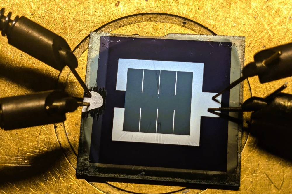
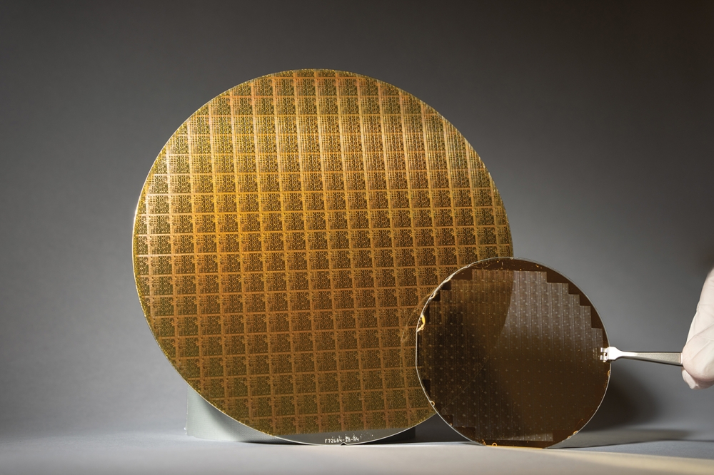
Researchers at the University of Southampton's Zepler Institute have successfully fabricated and characterised large-area 2D films of MoS2 at room temperature using a process which is scalable to any size wafer.
Previously only commercially available in small flakes, these wafer-scale films pave the way for the large-scale manufacture of a wide variety of devices including flexible and transparent optoelectronics, gas sensors, memory devices and photovoltaics (PV), according to the team.
Fabricated using ambient pressure CVD, the MoS2 films have an important advantage over other 2D materials like graphene: they enable the emission and detection of light.
MoS2 has exceptional carrier mobility and is believed to be a contender for the next generation of electronics which will soon take over as the silicon chip reaches its fundamental limits. In addition, MoS2 is an N-type semiconductor for PV applications.
By processing initially at room temperature, rather than at the high temperatures typically used (in the region of 800-900degC), it is possible to deposit MoS2 on a wider range of substrates, namely those with low thermal stability like flexible displays. The technique also minimises stress on other previously deposited layers and helps reduce processing costs.
"Using flakes of MoS2, which are typically only a few hundred square microns in area, to make devices is impractical time-consuming and inefficient and do not provide a practical route to rapid prototyping and existing semiconductor fabrication protocols. For these new materials to be adopted in mainstream electronics, they must be compatible with the semiconductor processing lines used in the mass production of electronic chips, " said Dan Hewak, professor of optoelectronics at the Zepler Institute.
"Our expertise in novel thin-film fabrication coupled with our ultra-high purity raw material processing facility has enabled us to purify and synthesise large area films to a consistency and purity level not available commercially."
The ambient pressure CVD process that Hewak and his colleagues have developed is an industrially-scalable and controllable deposition methodology and can be used to grow films on a variety of different substrates including plastic.
"We have also developed a technique for lifting these large-area films off the substrate they were grown on and depositing them onto a different substrate," said Hewak. "This means the films can be put onto any material, opening up entirely new applications."
Nanyang Technological University, Singapore has been using these films in its research for the past two years. "There have been extraordinary efforts devoted to the study of 2D materials, especially MoS2. For these materials to be useful in real applications and for many fundamental studies, the ability to fabricate uniform large-area thin films is critical. We are very pleased with the quality and uniformity of large-area CVD grown MoS2 thin films from Southampton which have helped us on the study of Ultrafast Carrier Thermalization and Cooling Dynamics in Few-layer MoS2. We are looking forward to further collaboration in this emerging 2D material at the device level", says Shen Ze Xiang, professor, program chair (sustainable earth), School of Physical and Mathematical Sciences, Nanyang Technological University.
Hewak and his colleagues are developing processes for the fabrication of a range of transition metal dichalcogenides and are part of the Chalcogenide Advanced Manufacturing Partnership (ChAMP). ChAMP is an EPSRC-funded partnership between five leading universities and 15 industrial partners dedicated to establishing the UK as a world leader in chalcogenide-glass technology through the development of advanced manufacturing techniques and practical application demonstrations.
"The significant breakthrough in large-area thin films of MoS2 is a very exciting development and Southampton's world leading capability presents the UK with unique opportunities for new devices and applications. The potential to integrate these new materials with existing semiconductors such as III-Vs is very attractive and we are keen to build collaboration and joint development in this area based on the new technology" says Jon Heffernan, director of the EPSRC National Centre for III-V Technologies at the University of Sheffield.


