
Refined reactors trim chip costs
Automated reactors that accommodate more wafers and in-situ cleaning drive down the cost of making wide bandgap devices for power electronics
BY CHRISTOPH GIESEN AND MICHAEL HEUKEN FROM AIXTRON
Designers of electrical systems are only going to embrace this new chip technology, however, if the total bill of materials is no higher when products are built with these superior components "“ and unfortunately, that's often not the case today. But this weakness associated with GaN and SiC diodes and transistors is being addressed, with these wide bandgap devices becoming increasingly competitive through efforts such as the Neuland project. Backed by €4.7 million of funding from the German Federal Ministry of Education and Research (BMBF), this project ran from 2011 to 2014 and involved Infineon Technologies, Aixtron, SiCrystal AG and SMA Solar Technology.
The Neuland project has taken a two-pronged approach to meeting its primary objective: the enhancement of SiC technology, with the aim of slashing costs via improvements in material quality, which ultimately spawn a hike in yield; and the development of a completely new power electronics technology
that is based on high-blocking vooltage GaN layers, which are grown on 200 mm silicon, a comparatively low-cost, large-scale substrate. These differing approaches are united by the same goal "“ to construct prototype diodes and inverters that deliver virtually loss-free switching and are capable of handling blocking voltages up to 1500 V and currents up to 10 A.
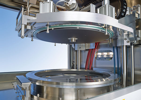
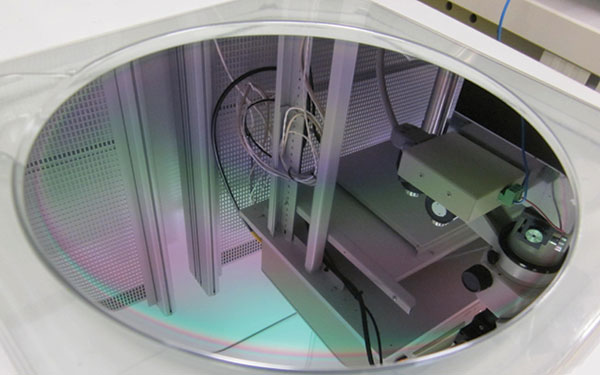
The reactor chamber of Aixtron's Planetary system AIX G5+ that can be used for the growth of GaN on 200 mm silicon substrates.
At Aixtron of Aachen, Germany, our role within the Neuland project has been to develop an MOCVD technology for the industrial production of GaN-based HEMT epistructures for power electronic devices. We have succeeded in this endeavour, creating a multi-wafer reactor that combines industry-leading throughput with a very high "˜up-time', thanks to in-situ cleaning and a high degree of automation.
Growing on siliconA lack of availability of large, low-cost native substrates dictates that the manufacture of GaN HEMTs will always involve the growth of epilayers on a foreign substrate. While sapphire substrates are widely used for making GaN LEDs, they are not suitable for power electronics, because they have a low thermal conductivity and can bend at the elevated temperatures used for growth. Note that even during pre-growth heating, 150 mm substrates can lift several millimetres off the edge of the reactor surface and even break.
Meanwhile SiC, while offering excellent thermal conductivity, is limited in size and very expensive. Consequently, it is an obvious choice to select silicon substrates for developing GaN HEMTs. This platform is mature, excellent in quality, available in diameters of up to 300 mm, and provides a thermal conductivity comparable to that of GaN.
However, despite all these attributes, silicon is not a perfect substrate. Instead, growth is very challenging, due to significant differences in the thermal expansion coefficients and lattice constants of the GaN-based layers and the silicon substrate. These differences are to blame for stresses within the material, which build-up during growth and can cause curvature of the wafers "“ and once they cease to have full contact with the susceptor, problems are compounded by an inhomogeneous temperature distribution. Making matters worse, these issues are magnified with increasing substrate diameter, and it is even possible for cracking to occur during wafer cooling.
Makers of GaN-on-silicon LEDs also face these issues, but at least they don't have to contend with additional problems stemming from the high aluminium content in the AlGaN films. Increasing aluminium content in ternary and quaternary material introduces more stress into the material, and also increases pre-reactions between the aluminium and nitrogen sources. The parasitic reactions that result are highly undesirable: They impair process efficiency, and they also introduce inhomogeneous depletion profiles that cause variations in material composition across the substrate. And on top of this, they can be a source of particles within the reactor. However, we have shown that by addressing all of these issues, it is possible to produce the form of AlGaN-based HEMT being developed in the Neuland project.
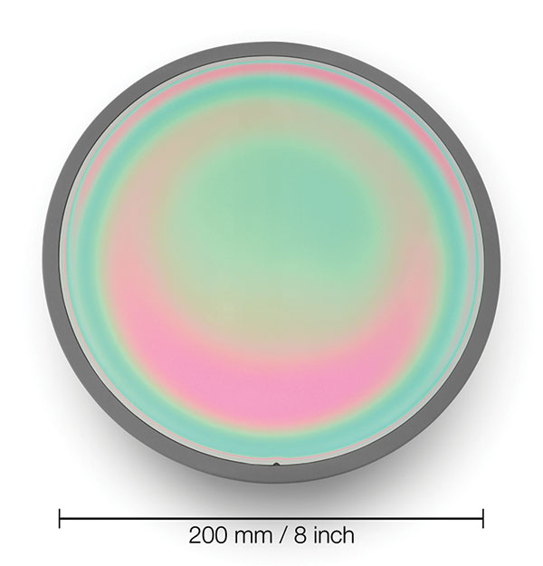
An epitaxial wafer manufactured with 5 x 200 mm AIX G5+ system
To make these HEMTs competitive with silicon equivalents, manufacturing costs must be as low as possible. The epitaxial growth process accounts for a significant proportion of chip costs, and to trim this we have investigated increasing the capacity of multi-wafer reactors, and refining the growth process as silicon substrate diameter increases from 100 mm to 150 mm and then 200 mm.
Efforts in this direction included the development of a 56 by 2-inch Planetary Reactor, based on our 42 by 2-inch (or 11 x 100 mm) reactor. This can also house either 14 wafers with a diameter of 100 mm, eight 150 mm wafers or five 200 mm wafers. Due to a lack of availability of industry-standard, high-quality, 2-inch silicon-substrates, we started development of our HEMT growth process on 100 mm wafers, before moving on to 150 mm and then 200 mm wafers.
Improvements to the hardware carried out during the Neuland project included optimisation of the susceptor, the exhaust collector (flow dynamics), the gas inlet (flow dynamics, uniformity, efficiency) and the ceiling (particles and temperature management). We also developed a new susceptor design for either eight 150 mm or five 200 mm wafers. This is compatible with automation, while guaranteeing an extremely uniform temperature distribution over large silicon substrates.
Part of this work involved the development of specific gas inlets for the 150 mm and 200 mm configurations to ensure extremely homogeneous and reproducible deposition of ternary and quaternary materials. Thanks to these new inlets, the growth window for depositing high quality layers significantly expanded.
In addition to these refinements, the other major breakthrough that we have made involves optimisation of the materials inside the reactor. This change reduced particle generation and extended the maintenance-free operation of the system.
Underpinning all of these changes to the design of our reactor were simulations that offered an insight into the impact of the new design on the deposition process. If these changes were positive, optimized parts were manufactured, implemented in the existing system and qualified for the process.
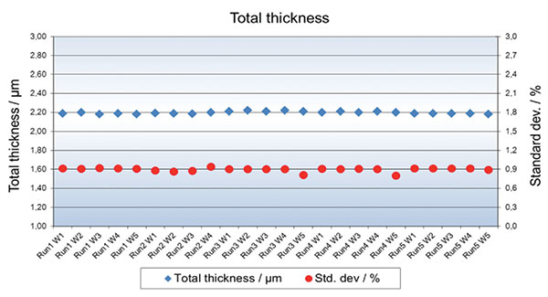
Run-to-run stability for mass production: Thickness uniformity for five full load runs using same HEMT recipe
We also developed an improved chemical model for the epitaxial growth of aluminium-based nitrides. This model considers parasitic gas phase processes that can occur in an MOCVD chamber, and it draws on an extensive experimental database that reveals how the chemical behaviour of AlGaN is influenced not only by general considerations, such as temperature
and partial pressure of the sources, but by the reactor design and the epitaxial process. Armed with all this information, we were able to make quicker progress as we refined our reactor's design.
Optimising temperature profilesUniform temperatures are critical to realising high-quality epiwafers. To excel in this regard, we simulated the influence of different reactor components on the temperature profile within the growth chamber. Following optimisation via simulations, components were designed, manufactured and subsequently tested in the laboratory. By optimising the satellite design, we could hit the target for temperature deviation, but the variation from satellite to satellite exceeded the specification. To meet this requirement, we then developed a technology allowing in-situadjustment of temperature deviations, and this enabled us to realise a ± 1 °C specification over all satellites.
Using this improved temperature uniformity, we manufactured HEMTs with an optimized technology on 150 µm substrates. These epiwafers exhibit state-of-the-art properties, with sheet resistance and breakdown voltages, measured in both the vertical and horizontal directions, comparable to those of commercial wafers from smaller reactors.
These epiwafers are also a success when viewed from another perspective − the targets set in the Neuland project. The goal of a mobility of 1600 cm2/Vs for a HEMT structure with a sheet carrier concentration of 1x1013 cm-2 was not only realised on 100 µm substrates, as intended, but also on 150 mm cousins. We were also able to produce non-passivated samples with an average electron mobility of 1700 cm2 V-1 s-1 at a carrier concentration of
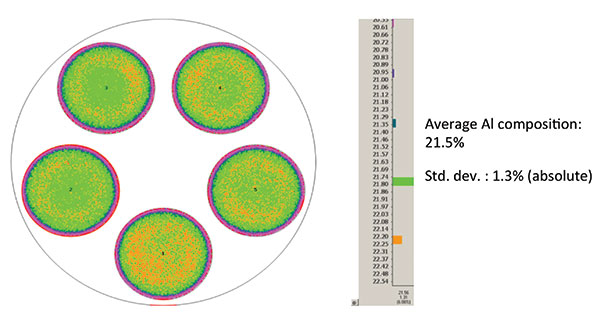
Aluminium concentration uniformity in the AlGaN barrier of a GaN-based HEMT structure formed on 200 mm silicon.
1.2 x 1013 cm-2, as well as crack-free, 6 µm-thick, highly resistive (>105 Ohm/sq.) buffer structures. And by employing the combination of an optimised reactor, epitaxy process and buffer structure, we could produce 200 µm epiwafers with a bow below 50 mm. This makes them flat enough to be processed in silicon lines.
To ensure that the production cost of these epiwafers is as competitive as possible, we have also looked at issues relating to throughput, such as the time taken for maintenance and fault fixing. This has led to increased automation, which can improve manufacturing efficiency.In-situ cleaning is a fundamental requirement for effective automation, and we have worked on this during and after the Neuland project.
The pay-off from in-situ cleaning is far greater than just the opportunity for increased automation, however. By ensuring equal starting conditions for every growth run, there are the promises of greater reproducibility and increased yield. What's more, in-situ cleaning can alleviate the need to change hardware between production runs, thereby reducing cycle times and eliminating potential operator errors. Spare-part costs should also fall, as well as the number of particles in the process.
The G5 seriesWe have used our findings from the Neuland project to enhance our G5 product family, especially the AIX G5+. This reactor, a Planetary system capable of housing five 200 mm wafers, was launched in July 2012 and it still setting the standard for the manufacture of power electronic devices based on GaN-on-silicon technology.
As well as this, the insights that we garnered during the Neuland project have enabled us to improve our G5 warm-wall system, which has been exclusively designed for SiC epitaxy. This reactor can process up to eight 150 mm SiC wafers, and combines the highest wafer throughput with the shortest cycle times and lowest cost of ownership.
Improvements to reactor design and process improvement didn't stop at the end of the Neuland project, but are on going, now being pursued as part of a project funded by the European Union called HiPoSwitch. This effort, which aims to deliver advances in GaN-based normally off high-power switching transistors for efficient power converters, includes an examination of the possibilities to upgrade the MOCVD production capacity and efficiency.
A 200 mm GaN-on-silicon HEMT epiwafer.
Through this and Neuland we have developed, in three steps, a full automated MOCVD tool that can accommodate five 200 mm wafers. The first of these steps involved optimisation of the reactor chamber to optimise growth on 200 mm substrates, and this was followed by implementation and optimization of the pre-developed in-situ reactor cleaning process to cut maintenance time between growth runs. The latter step enabled fully automatized cassette-to-cassette wafer handling, leading to a superior growth tool that has been qualified for the HEMT process.
Thanks to these developments, this reactor and its sibling for SiC growth are currently the most advanced systems for the volume production of power devices.


