On-resistance falls for vertical GaN MOSFETs
Vertical GaN MOSFETs with a hexagonal layout are now meeting the requirements for automotive applications
Researchers from Toyoda Gosei are claiming to have set a new benchmark for the performance of a vertical GaN MOSFET with a device that has an on-resistance of just 1.8 mΩ cm2.
Not only does this 1.2 kV device better the on-resistance of other vertical GaN MOSFETs, which have realised on-resistances as low as 2-3 mΩ cm2 "“ it also breaks new ground by delivering the blocking voltages and threshold voltages required for use in high-power automotive applications.
Threshold voltages of 3-5 V are preferred for this application, in order to prevent false operation caused by factors such as noise. The team's vertical MOSFET meets this requirement, having a threshold voltage of 3.5 V, while the more common lateral GaN transistors can rarely meet this need.
Another weakness of lateral GaN transistors is that in order to deliver a high breakdown voltage they must have a substantial gate-drain spacing, and this drives up the size and cost of the device. In comparison, with vertical transistors, an increase in thickness of the drift region leads to a higher breakdown voltage, with chip size remaining the same.
Back in 2014, the Toyoda Gosei team claimed a record-breaking blocking voltage of 1.6 kV for a GaN-based trench MOSFET. Their latest device is based on this.
"We redesigned thicknesses and doping concentrations of channel and drift layers to reduce the resistances of the epitaxial layers while maintaining a blocking voltage over 1.2 kV," explains Tohru Oka, corresponding author of the paper. "Furthermore, we adopted a regular hexagonal shaped trench gate layout to increase a gate width per unit area, to effectively reduce the specific on-resistance."
Devices were formed on a n-type GaN substrate with a doping concentration of 1 x 1018 cm-3 and a dislocation density of 106 cm-2. MOCVD created the epitaxial structure, which consisted of: a 13 µm-thick layer of n-type GaN with a silicon doping concentration of 9 x 1015 cm-3; a 0.7 mm-thick layer of p-type GaN, magnesium-doped to a concentration of 2 x 1018 cm-3; and a 0.2 µm-thick layer of n-type GaN with a silicon doping concentration of 6 x 1018 cm-3.
Inductively coupled plasma etching with chlorine gas defined the isolation mesa, recess regions for p-body contacts and gate trenches. Atomic layer deposition then added an 80 nm-thick SiO2 film that provided the gate dielectric, with palladium providing the p-body electrode, and an Ti/Al stack employed for the source and drain electrodes. To minimise the separation of the centres of the source electrodes, they are stacked on the p-body electrodes.

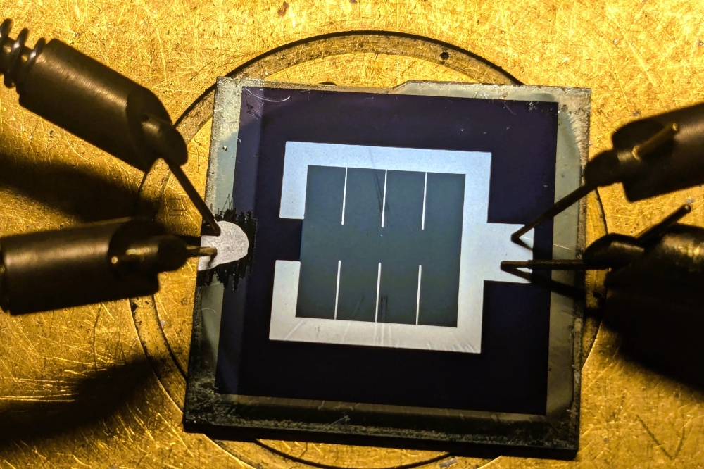
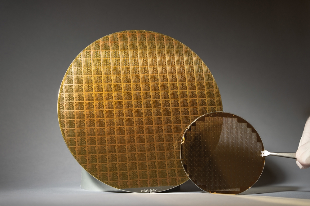
Vertical GaN MOSFETs developed by Toyoda Gosei are delivering the blocking voltages, threshold voltages and specific on-resistances required for automotive applications.
The team annealed the devices under nitrogen gas for 5 minutes at 550 °C. Interlayer dielectrics were formed from a 100 nm-thick layer of Al2O3, added by atomic layer deposition, and an 800 nm-thick film of SiO2 that was deposited by plasma-enhanced CVD. To reduce the potential for crowding at the edge of the p-n junction around the isolation mesa periphery, engineers turned to field-plate edge termination in the vicinity of the isolation mesa periphery.
One of the merits of using hexagonal cells, rather than stripe cells, is that they can double the ratio of gate width to unit cell area. This is highly beneficial, leading to an increase in current density and a trimming of specific on-resistance.
Electrical characterisation of the vertical MOSFETs revealed a blocking voltage of 1.2 kV, and a current density per unit gate length of 10.2 A/mm at a gate voltage of 40 V. This current density is more than three times that of the previous device at the same gate bias electric field, and is attributed to reductions in channel and drift resistance that result from redesigning the thickness and doping concentrations of channel and drift layers.
The on-resistance of the latest device, 1.8 mΩ cm2, is a factor of 6.6 less than that of its predecessor. The improvement results from an increase in current density by a factor of 3.3, and the doubling of the ratio of gate width to unit cell area.
Oka says that the team will now use the developed technologies to work towards the practical use of power devices.


