Loading...
News Article

Peregrine Introduces First RF SOI 300mm platform

News
Globalfoundries and Peregrine collaborate to achieve an industry first with  UltraCMOS

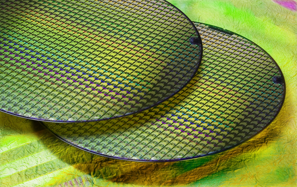
Peregrine Semiconductor, known for its RF SOI (silicon on insulator) technology, has announced the UltraCMOS 11 platform, the first RF SOI technology built on Globalfoundries' 130nm 300mm RF technology platform. 

Moving to a 300mm wafer, Peregrine says, opens the door to new enhancements and advanced features in future generations of the UltraCMOS technology platform, which can use Globalfoundries' 300mm production-proven design and manufacturing expertise.

 "As an industry first, the new RF SOI technology reaffirms our commitment to the RF market, and is another example how Globalfoundries' 300mm fab in Singapore can provide new levels of performance, reliability and scalability for integrated RF front-end solutions," said Brian Harrison, senior vice president of Integration and Factory Management at Globalfoundries. "We are pleased to see the tremendous efforts resulted in this achievement, and we will continue to leverage our RF process development expertise and manufacturing scale to maximise the technology's capabilities and drive differentiation with our customers."

The UltraCMOS 11 platform will be the foundation for Peregrine's high volume mobile products and SOI products for other applications. It builds on the success of the UltraCMOS 10 technology platform, also developed and manufactured by Globalfoundries. 

 "For over 25 years, Peregrine has been at the forefront of advancing RF SOI technology," said Jim Cable, CEO of Peregrine Semiconductor. "That legacy continues with today's introduction of the UltraCMOS 11 platform, the first RF SOI 300 mm technology platform. By using 300 mm wafers, Peregrine ensures our technology roadmap will continue to be on the leading edge of RF SOI."

New efficiency record for CIGS perovskite tandem cells
Realising tuneable InGaN laser diodes
SiC patenting strong in Q4 2024, says KnowMade
Say hello to the heterogeneous revolution
Double heterostructure HEMTs for handsets
AlixLabs to collaborate with Linköping University
Multiple materials vie for RF success
SiC MOSFETs: Understanding the benefits of plasma nitridation
Wolfspeed reports Q2 results
VueReal secures $40.5m to scale MicroSolid printing
Mitsubishi joins Horizon Europe's FLAGCHIP project
Vishay launches new high voltage SiC diodes
UK team leads diamond-FET breakthrough
GaN adoption at tipping point, says Infineon
BluGlass files tuneable GaN laser patents
QD company Quantum Science expands into new facility
Innoscience files lawsuit against Infineon
Riber revenues up 5% to €41.2m
Forvia Hella to use CoolSiC for next generation charging
Photon Design to exhibit QD simulation tool
Ortel transfers CW laser fabrication to Canada
Luminus adds red and blue multi-mode Lasers
PseudolithIC raises $6M for heterogeneous chiplet tech
Mesa sidewall design improves HV DUV LEDs
IQE revenue to exceed expectations
'Game-changing' VCSEL system targets clinical imaging
German start-up secures finance for SiC processing tech
Macom signs preliminaries for CHIPS Act funding
IQE and Quintessent partner on QD lasers for AI
EU funds perovskite tandems for fuel-free space propulsion
EU to invest €3m in GeSi quantum project
Transforming the current density of AlN Schottky barrier diodes
×
Search the news archive

To close this popup you can press escape or click the close icon.
Logo
x
Logo
×
Register - Step 1

You may choose to subscribe to the Compound Semiconductor Magazine, the Compound Semiconductor Newsletter, or both. You may also request additional information if required, before submitting your application.


Please subscribe me to:


You chose the industry type of "Other"

Please enter the industry that you work in: