First fully depleted 22nm SOI wafers come to market
Strong industry support now includes extended IP and design services as well as multiple substrate suppliers, ensuring high-volume manufacturing capacity
Globalfoundries has announced the industry' first 22nm fully depleted (FD) silicon-on-insulator (SOI) technology platform which it is calling 22FDX.
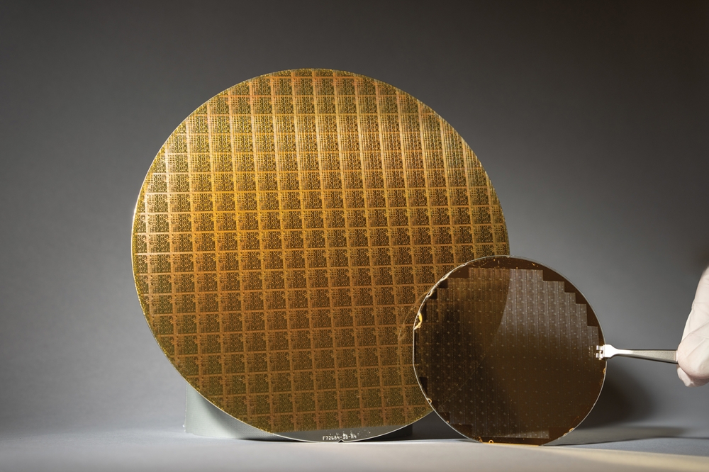
The FD-SOI process technologies are based on ultra-thin SOI substrates manufactured using French firm Soitec's industry-standard Smart Cut technology. Soitec's 300mm FD-SOI substrates are ready now for ramp-up production with the capacity to meet industry forecasts, from the company`s two large 300mm facilities in Europe and Singapore.
An additional volume of identical substrates will be available from the silicon-wafer world leader Shin-Etsu Handotai(SEH), a Smart Cut licensee. Both wafer suppliers are reportedly ready to increase capacity as needed.
The news is said to represent a major step in the FD-SOI roadmap for 22nm processing. According to Globalfoundries, its 22FDX technology will offer significant performance and cost benefits for applications demanding low-power and high-performance requirements with possible analogue and RF integration. The technology is ideal for the low to mid-range mobile and wearable device markets, while enabling a new generation of system-on-chip (SOC) technologies for the rapidly evolving Internet of Things (IoT). Other markets include consumer multimedia, industrial and automotive applications.
"Globalfoundries' announcement is a key milestone for enabling the next generation of low-power electronics and we are very pleased to be Globalfoundries` strategic partner," said Paul Boudre, CEO of Soitec.
"Our ultra-thin SOI substrate is ready for high-volume manufacturing of 22FDX technology. With our two fabs and our worldwide licensing strategy, the market will enjoy all of the SOI wafers it needs for strong adoption. The markets we are addressing with this product will be key contributors to Soitec`s growth."
"SEH welcomes this development, bringing FD-SOI products to the industry, and we look forward to the continuation of our work in extending the global supply chain for FD-SOI," said Nobuhiko Noto, general manager of SOI Division at SEH. "We are very glad to be engaged in supporting the growth and development of the FD-SOI market, both as a leading bulk wafer supplier to Soitec as well as with our own FD-SOI wafer supply."
The performance, power consumption, and cost benefits of FD-SOI have been proven, and FD- SOI is expected to go into a high-volume production phase. According to Handel Jones, CEO of IBS, Inc. "Multi-source supply chain for substrates has been established, and wafer volumes can potentially be one million per year and more in the future. We are confident that Soitec and its licensing strategy will be able to supply the substrates required to allow FD-SOI wafer volumes to reach their potential."
The global FD-SOI ecosystem continues to grow with the participation of more leading semiconductor foundries. In May 2014, Samsung announced the signing of a comprehensive agreement with STMicroelectronics on 28nm FD-SOI technology for multi-source manufacturing collaboration.


