AlN Schottky barrier diode makes its debut
HVPE growth enables the fabrication of Schottky barrier diodes with a bandgap of 6.1 eV
A team of researchers based in Japan and the US is claiming to have fabricated the first vertical Schottky barrier diodes made from AlN.
These devices promise to deliver a superior performance to existing wide bandgap devices, due to their much higher bandgap that leads to a far higher electric breakdown field. The bandgap of AlN is 6.1eV, and it has a breakdown electric field of 11.7 MV/cm, compared to 5.6 MV/cm for diamond, 3.3 MV/cm for GaN and between 2.0 MV/cm and 2.4 MV/cm for SiC.
Up until now, unlocking the potential of AlN Schottky barrier diodes has been held back by the lack of a suitable, native substrate. Electronic devices such as diodes require n-type conductivity, and this has been realised previously by either using oxygen impurities or nitrogen vacancies − or by turning to growth of films by MOCVD, which allows silicon doping, but film thicknesses tends to be less than 1µm. A more suitable approach is to deposit films using a faster deposition technique, HVPE. This is the approach taken by the Japan-US collaboration, which involves researchers from Tsukuba Research Laboratories, Fuji Electric Company, Tokyo University of Agriculture and Technology, HexaTech and North Carolina State University.
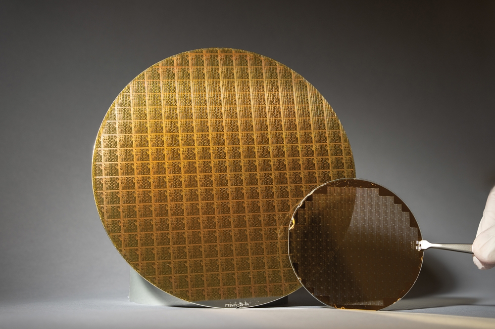
Members of this team produced substrates by growing, via HVPE at 1450degC, silicon-doped AlN layers up to 250µm-thick on chemically mechanically polished aluminium-polar surfaces. These surfaces were produced on highly insulating, 15mm-diameter AlN(0001) substrates that had been formed by physical vapour transport (PVT). Growth of the AlN proceeded at 25µm/hr, with quartz fragments placed on the susceptor providing a silicon dopant source.
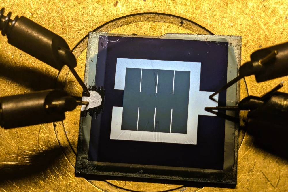
Devices were formed by chemical-mechanical polishing of the surface of the epilayer of AlN, and removal of the PVT-grown substrate to leave a 150µm-thick piece of freestanding AlN. Schottky contacts with dimensions of 270 µm by 270 µm were created by depositing 20nm of nickel and 50nm of gold on the N-polar surface.
X-ray diffraction offered an insight into the crystal quality of the free-standing AlN. Narrow peaks in the spectra indicated that the crystal quality is comparable to that of the PVT-grown AlN.
Secondary ion mass spectrometry revealed the dopants and the impurity levels in the HVPE-grown substrate. "The silicon concentration was 3à—1017 cm-3, and carbon and oxygen were below the detection limit," explains Toru Kinoshita from Tsukuba Research Laboratories.
To determine the electrical properties of the silicon-doped AlN, the team also grew a thinner film that would avoid a measurement error caused by thickness inhomogeneity. Measurements on the resulting 32 µm-thick film at 300K revealed a net electron concentration of 2.4 x 1014 cm-3, a mobility of 115 cm2 V-1s-1, and a resistivity of 2.3 x 10² Ω cm.
Compared to an AlN film grown by MOCVD, which had a similar silicon-doping concentration, the HVPE-film had a lower mobility. This might be surprising, since the HVPE-grown material had a dislocation density that is lower by four orders of magnitude "“ but it is plagued by a high total defect concentration, which the team blames for the low mobility.
Kinoshita and co-workers have studied the electrical properties of the device after gluing the substrate onto an AlN carrier with silver paste.
Measured at 298 K, the Schottky barrier diode had a turn-on voltage of 2.2V, a series resistance of 3.5 x 10⁶ Ω, and an ideality factor of 7.9. Using a thermionic emission model and electrical data at various temperatures, the researchers estimated a barrier height for this device of 1.1eV at 298K.
The researchers believe that damage is present at the interface between the Schottky contact and the HVPE-grown AlN, resulting from mechanical polishing. This is to blame for the high ideality factor and the large difference between the barrier height and the turn-on voltage.


