Double miscut substrates yield superior quantum wells
Narrower, longer emission results from growth on m-plane substrates with a second miscut
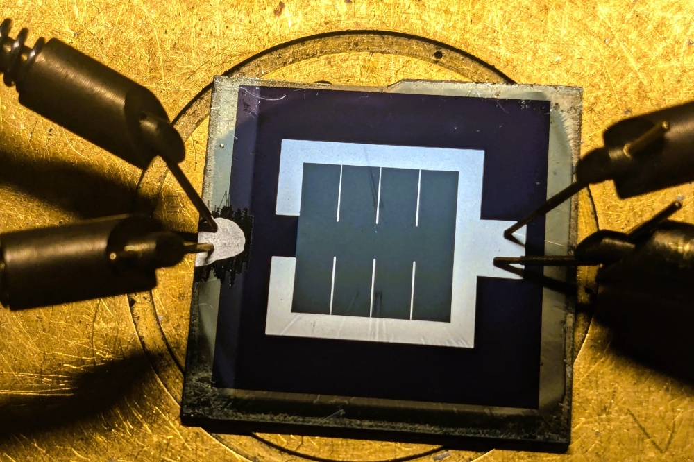
Researchers at the University of California, Santa Barbara (USCB), have improved the characteristics of m-plane InGaN quantum wells by growing these heterostructures on substrates that are miscut in two directions.
The superior quantum wells promise to improve the performance of m-plane laser diodes. These devices have an inherent advantage over the more conventional c-plane lasers, which are held back by internal electric fields that hamper radiative recombination. However, the m-plane variants suffer from a broad line width that lowers the peak power in the spontaneous emission spectrum.
The West-coast team has shown that it is possible to address this by turning to double miscut substrates "“ they are miscut along the a- and c-directions. Quantum wells formed on this foundation, which is provided by the Mitsubishi Chemical Company, produce improved spontaneous emission characteristics.
Interest in miscut substrates for m-plane growth is not new. As far back as 2007 researchers from UCSB were reporting results on substrates with a -1° miscut in the c-direction. That platform for growth supresses the formation of hillocks that would occur on on-axis, m-plane substrates.
Compared to c-plane substrates, single miscut m-plane variants exhibit a low indium uptake and lead to quantum wells with a broad luminescence linewidth. Both of these weaknesses hamper the fabrication of high-performance lasers: Broad luminescence distributes carriers over many non-lasing optical modes, leading to a lower peak power and peak gain; and a reduction in indium uptake has to be compensated for by lowering the growth temperature "“ and this degrades the crystal quality of the heterostructure.
Atomic force microscopy images expose the superior growth of heterostructures on m-plane substrates that have a miscut in two directions
A previous study by UCSB found that quantum wells grown on substrates that are -1° miscut in the c-direction have a striated morphology, with striated regions exhibiting emission at longer wavelengths. These striations are formed from a diagonal stepflow, with a directional component along the a- and c-axis that led to increased indium content.
This observation encouraged growth of quantum wells on double-miscut substrates. This latest study involved co-loading substrates into an MOCVD reactor that had either a miscut of -1° in the c-direction or two miscuts: either a miscut of 1.49° in the c-direction and a miscut of 2.10° in the a-direction; or a miscut of 0.21° in the c-direction and 0.51° in the a-direction.
On all these substrates the researchers grew a range of LED and laser stuctures at 1100degC. They featured one to three wells with widths of 4nm to 12nm, separated by quantum barriers with widths of 8nm to 16nm.
Atomic force microscopy images of the heterostructures grown on the double miscut substrates revealed stable step-flow growth, with straight edges and a constant terrace width.
The researchers performed on-wafer electroluminescence measurements on many of the heterostructures, using 0.1 mm2 indium p-type contacts and n-contacts formed by soldering indium to the wafer edge. LEDs with a double miscut of 1.49° in the c-direction and a miscut of 2.10° in the a-direction produced longer emission wavelengths for fluorescence, phtotoluminecence and electroluminescence. For the latter, the emission peak of an LED red-shifted by 38 nm compared to that formed on a miscut of -1° in the c-direction, thanks to higher indium uptake.
Another strength of the double-miscut substrates is narrower emission. Electroluminescence of laser diode structures revealed a full-width at half maximum of 30.5 nm for a structure grown on a substrate with a miscut of 1.49° in the c-direction and a miscut of 2.10° in the a-direction. This is 14.4 nm narrower than that for a laser on a substrate with a miscut of -1° in the c-direction.
The team told Compound Semiconductor that they are now planning to make lasers. They are currently developing epitaxial and processing steps, and will soon compare the performance of lasers grown on different miscuts.


