
II-VI Advanced Demonstrates First 200mm SiC Wafer
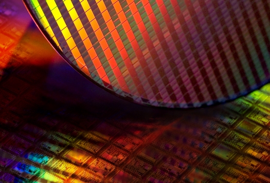
II-VI Advanced Materials, a US supplier of single crystal SiC substrates and CVD-grown polycrystalline diamond materials, recently exhibited the world's first 200mm diameter SiC wafer at the 2015 Compound Semiconductor Manufacturing Technology (CS MANTECH) conference in Scottsdale, AZ and the International SiC Power Electronics Applications Workshop (ISiCPEAW) in Stockholm, Sweden.
Thomas Anderson, general manager of II-VI Advanced Materials said: "The earlier introduction of our 150mm diameter SiC substrates was extremely well received by our customers, and significant growth in the demand reflects market recognition of the improved economics of SiC device manufacturing at increased diameters. Devices built on these substrates will be or are currently being utilised in a wide range of applications requiring high power density and system efficiency, such as electric vehicles, inverters for PV solar energy and other renewable energy installations."
This development program builds upon years of work funded, in part, by the US Air Force Research Laboratory (AFRL). It focused on the manufacturing scale-up of the II-VI Advanced Physical Vapour Transport (APVT) SiC crystal growth technology as well as the development of state-of-the-art fabrication, polishing and cleaning processes. These efforts have resulted in achievement of world-class quality material, according to the company, while at the same time increasing the diameter from 3in to 100mm, then to 150mm and now to the world's first 200mm SiC substrates.
"This 200mm SiC wafer demonstrates our market leading crystal growth and fabrication technologies, as well as our commitment to respond to and work with our customers to ensure a smooth transition to the next generation of substrates. We are dedicated to pushing the boundaries of SiC substrate technology to ensure that the market has the material it needs to make high performance SiC based devices both cost effective and widely utilised," commented Andrew Souzis, director of business development.


