
Big wafers, grand designs
With recent investment funds, Exagan is getting ready to market GaN-on-silicon FETs on 200 mm wafers. Compound Semiconductor reports.
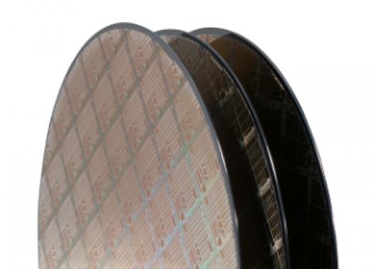
Exagan is fabricating its first GaN-on-silicon devices on 200 mm, rather than 150 mm, wafers.
As investment into GaN power semiconductors gathers momentum, France-based Exagan, is one of a raft of companies to receive funds.
Raising €5.7 million in June, this year, the fabless Leti-Soitec spin-out joins the likes of Transphorm, US and GaN Systems, Canada, now pumped up to produce power switching devices for photovoltaic, automotive and PC markets.
But unlike its contemporaries, Exagan intends to fabricate its first market-ready GaN-on-silicon devices on 200 mm, rather than 150 mm, wafers.
"By fabricating devices on 200 mm wafers, you reduce the processing costs, increase device yields but the biggest benefit is accessing the CMOS technology and manufacturing that exceed 150 mm [wafer sizes] capabilities," explains Frédéric Dupont, president and chief executive of Exagan.
"You have access to a wider portfolio of technology and this all increases the attractiveness of GaN devices," he adds.
Exagan has already fabricated its first prototype 650V FETs on 200 mm wafers, working with engineers at X-FAB Silicon Foundries' CMOS wafer fab in Dresden, Germany. The fabless French start-up now intends to use the latest cash injection to industrialise these products.
According to Dupont, his company will now increase device quality and reliability, and deliver initial samples to customers by the end of this year.
"Looking at what the competition is doing, we believe there is still some work to be done on device reliability to meet market requirements at the right cost," he says. "This is why we're pursuing our 200 mm strategy and we intend to deliver the same quality and reliability of silicon devices, as requested by customers."
"GaN devices operate at much faster frequencies than silicon devices so characterising these devices is a challenge," he adds. "But we have very talented power engineers in our team, to address those challenges."
Secure supply chains
From word go, a critical part of Exagan's commercialisation strategy has been to secure a robust supply chain for GaN-on-silicon power devices, and so become Europe's primary supplier of GaN-based power switches.
According to Dupont, epitaxy is licensed from Soitec and will be retained within Exagan's own materials facility. XFAB will carry out all device processing, and partnerships are already formed for device testing.
"As well as smaller companies such as ourselves, and say EPC, we have some very big players in this market including International Rectifier that became Infineon," he highlights. "But I think it is important for new entrants like us to have a place in this market as we are bringing some flexibility and we are going to be pushing the technology very aggressively."
"The larger players are developing a broad product portfolio with alternative technology such as silicon carbide," he adds. "But we'll be pushing GaN-on-silicon vigorously and once our devices are qualified, customers will know there is no limitation to ramping up volumes."
Exagan's initial customers for its 650V FETs are likely to be manufacturers of inverters for photovoltaic and electric vehicle applications as well as power supply and power factor correction players, keen to move away from the silicon IGBT. Devices will be offered as dies or with standard packages in a first step.
But what about rival technology SiC? The PV inverter sector has already started to embrace qualified SiC Schottky Diodes and MOSFETs and more markets will follow.
Like the silicon IGBT, these transistors are normally-off devices, so replacing one device for the other, within a power system, is relatively straightforward. In contrast, the normally-on GaN-on-silicon FET demands different drivers and a system re-design.
To counter this, many GaN-on-silicon manufacturers are busy re-configuring the GaN HEMT as a normally-off device. Exagan is also developing normally-off approaches, but first products will be normally-on devices.
Dupont will not be drawn on applications or markets, but is quite clear that he does not see SiC devices as being a threat to GaN-on-silicon FETs.
"SiC has a clear advantage in terms of maturity, its proven and devices have reliability data," he says. "But for GaN-on-silicon, you're using silicon, you're using epi-reactors that can be bought everywhere and there's hundreds of fabs that can produce GaN-on-silicon at 200 mm."
"We will achieve the same performance as SiC devices, and then GaN will win because of the costs," he concludes.


