
IQE named as partner in US Photonics Institute
IQE, a supplier of advanced semiconductor wafers, has been announced as a key partner in a new consortium to establish the United States' first Integrated Photonics Institute for Manufacturing Innovation (IP-IMI).
Created as part of President Obama's National Network for Manufacturing Innovation (NNMI), the IP-IMI was launched this week in Rochester, NY by US Vice President Biden as the sixth of nine new manufacturing institutes designed to bring industry together with academia and government to advance the state-of-the-art in the design, manufacture, testing, assembly, and packaging of photonic integrated circuits.
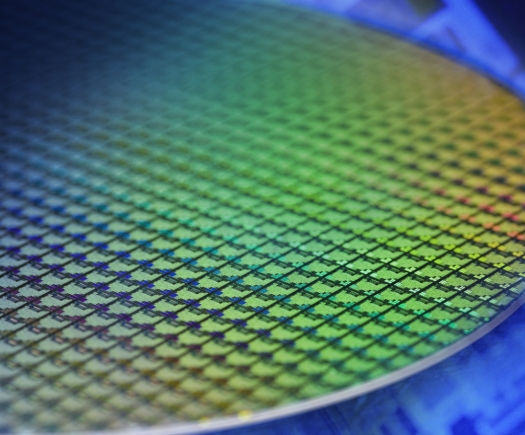
The consortium comprises 55 industrial partners, including Intel, IBM, Infinera, HP, Honeywell, Rockwell, Seagate and TI along with numerous other leading edge companies, universities and laboratories, and is led by the Research Foundation of the State University of New York (SUNY). IQE's role in the consortium is to provide advanced epitaxy services to the Institute partners.
Drew Nelson, IQE CEO and president said:"IQE is proud to have been named as one of 55 key industrial partners in this important project led by SUNY to accelerate photonic capabilities and manufacturing in the US.
"The importance of the rapidly growing photonics technology industry cannot be overestimated and is already having a major impact in areas such as communications, energy efficiency, healthcare and safety and security systems.
"Inclusion as a key partner in this new US Manufacturing Institute is testament to IQE's reputation as a global world leader in compound semiconductor materials, a key enabling technology (KET) for photonics."
The IP-IMI has been awarded federal funding of $110 million by the Department of Defense, which is expected to yield total public-private investment of more than $610 million which will enable the institute to focus on developing an end-to-end integrated photonics ecosystem in the US, including domestic foundry access, integrated design tools, automated packaging, assembly and test, and workforce development.
The Institute will develop and demonstrate innovative manufacturing technologies for ultra-high-speed transmission of signals for the internet and telecommunications; new high-performance information-processing systems and computing; compact sensor applications for medical advances in diagnostics and treatment; multi-sensor applications including urban navigation, free space optical communications and quantum information sciences; and other diverse military applications including electronic warfare, analogue RF sensing, communications, and chemical/biological detection.
All of these developments will require cross-cutting disciplines of design, manufacturing, packaging, reliability and testing.
The institute will provide central facilities through which academia, SMEs and large corporations can access latest technology for design and manufacture of photonics devices providing a route to commercialisation through high-value, high-volume manufacturing.


