Imec opens up GaN research initiative

Belgian nano-electronics research centre Imec is extending its GaN-on-Si R&D program, and is now offering joint research on GaN-on-Si 200mm epitaxy and enhancement mode device technology.
The extended R&D initiative includes exploration of novel substrates to improve the quality of the epitaxial layers, new isolation modules to increase the level of integration, and the development of advanced vertical devices. Imec welcomes new partners interested in next generation GaN technologies and companies looking for low-volume manufacturing of GaN-on-Si devices to enable the next generation of more efficient and compact power converters.
"Since the program's launch in July 2009, we have benefited from strong industry engagement, including participation from IDMs, epi-vendors and equipment and material suppliers. This underscores the industrial relevance of our offering," stated Rudi Cartuyvels, executive vice president of smart systems at Imec. "Interested companies are invited to become a partner and actively participate in our program. Imec's open innovation model allows companies to have early access to next-generation devices and power electronics processes, equipment and technologies and speed up innovation at shared cost."
GaN technology offers faster switching power devices with higher breakdown voltage and lower on-resistance than silicon, making it an outstanding material for advanced power electronic components. Imec's R&D program on GaN-on-Si was launched to develop a GaN-on-Si process and bring GaN technology towards industrialisation.
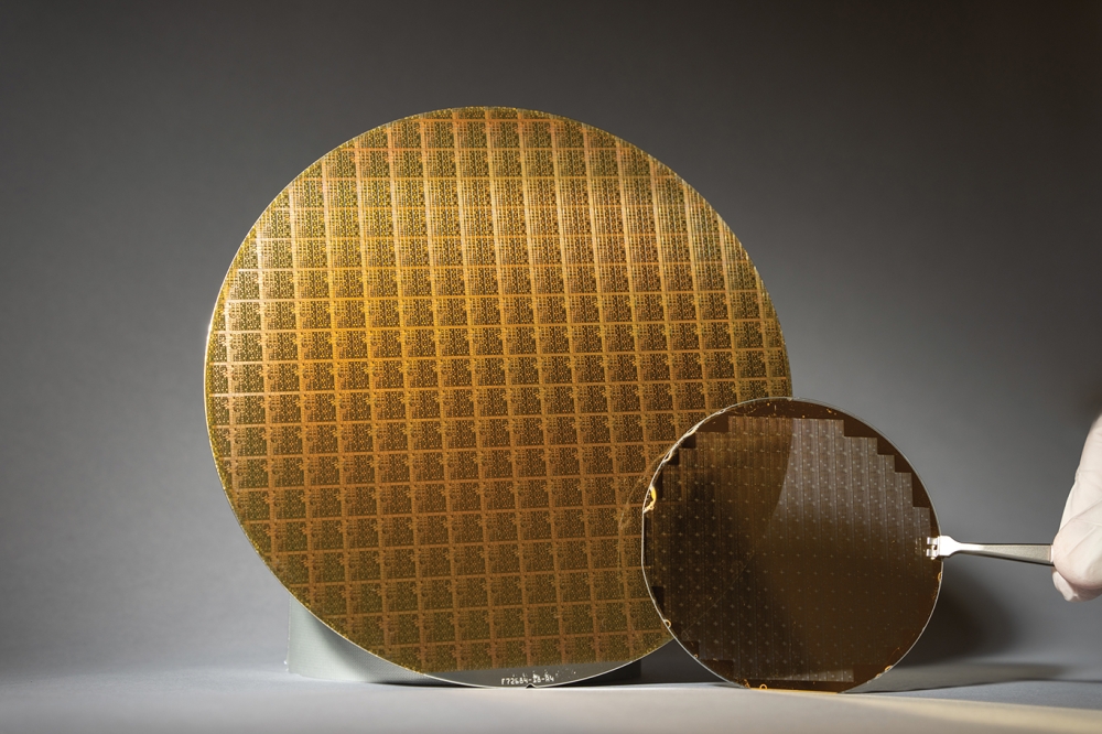
Building on Imec's track record in GaN epi-layer growth, new device concepts and CMOS device integration, imec has now developed a 200mm CMOS-compatible GaN process line. Imec's GaN-on-Si technology is reaching maturity, and companies can gain access to the platform by joining imec's GaN-on-Si industrial affiliation program (IIAP). The process line is also open to fabless companies interested in low-volume production of GaN-on-Si devices tailored to their specific needs, through dedicated development projects.
Imec's portfolio includes three types of buffers optimized for breakdown voltage and low traps-related phenomena (i.e. current dispersion): a step graded AlGaN buffer, a super lattice buffer, and a buffer with low-temperature AlN interlayers. Imec explored side-by-side enhancement mode power devices of the MISHEMT and p-GaN HEMT type, as well as a gate-edge terminated Schottky power diode featuring low reverse leakage and low turn-on voltage.
The latest generation of imec enhancement mode power devices shows a threshold voltage beyond +2V, an on-resistance below 10 ohm mm and output current beyond 450 mA/mm. These devices represents the state of the art of enhancement mode power devices.
In this next phase of the GaN program, imec is focusing on further improving the performance and reliability of its current power devices, while in parallel pushing the boundaries of the technology through innovation in substrate technology, higher levels of integration and exploration of novel device architectures.


