Loading...
News Article

GaN-on-silicon transferred to Epistar

ALLOS Semiconductors' mature 150 and 200mm technology now established

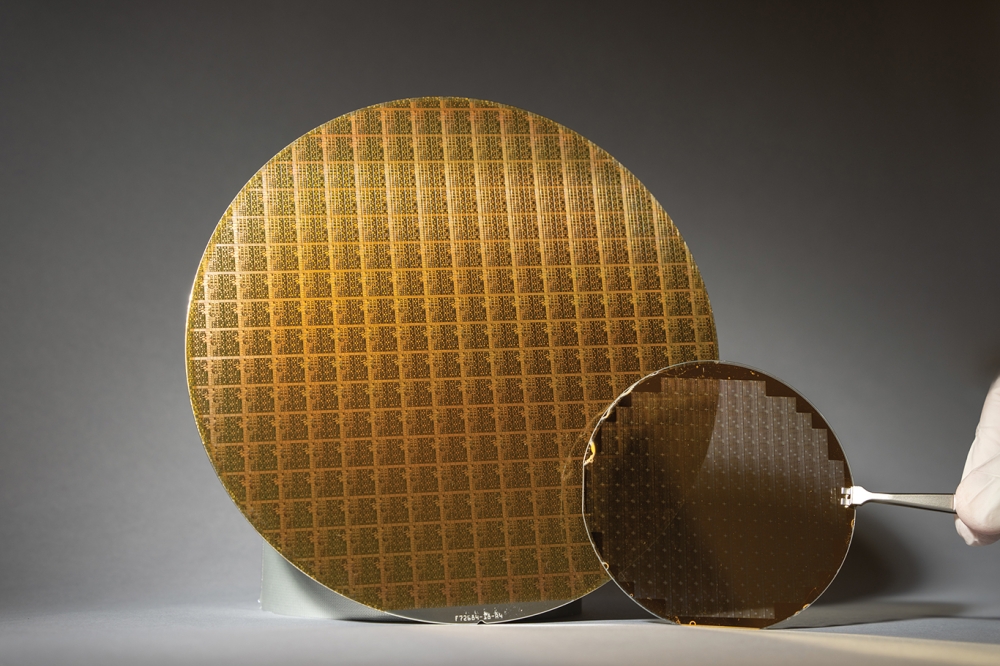
Taiwanese LED company Epistar and the German technology engineering and licensing company ALLOS Semiconductors have announced the successful conclusion of their project to establish ALLOS' mature 150 and 200mm GaN-on-Si technology at Epistar.

The project was carried out with better than expected results and ahead of schedule (in less than six months) according to the companies. For example reproducible crystal quality was achieved with total dislocation density value of 2x108cm2. With this performance Epistar says it has caught up with companies that have been developing GaN-on-Si LED technology for a long time.

During the project ALLOS established its GaN-on-Si epiwafer process on Epistar's epitaxy reactors. Epistar engineers were trained and worked in the integrated project team with ALLOS to gain full understanding and control over the GaN-on-Si technology. Currently Epistar's own leading LED technology is been transferred to GaN-on-Si structures.

"To conduct the technology transfer with ALLOS has proven to be the right decision for Epistar as it allowed us to quickly gain command over their leading GaN-on-Si technology in a very cost-efficient and reliable way", says  M. J. Jou, president of Epistar. He continues: "In a second phase we will now be focusing on realising the cost advantages of GaN-on-Si LEDs and to unlock the application benefits."

"To accomplish a project of this size and complexity with such results is a complete success and a good reason to be proud of the teams from both parties", comments Burkhard Slischka, CEO and co-founder of ALLOS. 

He further explains: "This result underlines ALLOS' project execution skills as well as our technical capabilities to grow crack free wafers with market leading crystal quality. This is an example that our fast, cost-effective and successful implementation of GaN-on-Si helps our customers to reduce development risk and to save time and money."

New efficiency record for CIGS perovskite tandem cells
Realising tuneable InGaN laser diodes
SiC patenting strong in Q4 2024, says KnowMade
Say hello to the heterogeneous revolution
Double heterostructure HEMTs for handsets
AlixLabs to collaborate with Linköping University
Multiple materials vie for RF success
SiC MOSFETs: Understanding the benefits of plasma nitridation
Wolfspeed reports Q2 results
VueReal secures $40.5m to scale MicroSolid printing
Mitsubishi joins Horizon Europe's FLAGCHIP project
Vishay launches new high voltage SiC diodes
UK team leads diamond-FET breakthrough
GaN adoption at tipping point, says Infineon
BluGlass files tuneable GaN laser patents
QD company Quantum Science expands into new facility
Innoscience files lawsuit against Infineon
Riber revenues up 5% to €41.2m
Forvia Hella to use CoolSiC for next generation charging
Photon Design to exhibit QD simulation tool
Ortel transfers CW laser fabrication to Canada
Luminus adds red and blue multi-mode Lasers
PseudolithIC raises $6M for heterogeneous chiplet tech
Mesa sidewall design improves HV DUV LEDs
IQE revenue to exceed expectations
'Game-changing' VCSEL system targets clinical imaging
German start-up secures finance for SiC processing tech
Macom signs preliminaries for CHIPS Act funding
IQE and Quintessent partner on QD lasers for AI
EU funds perovskite tandems for fuel-free space propulsion
EU to invest €3m in GeSi quantum project
Transforming the current density of AlN Schottky barrier diodes
×
Search the news archive

To close this popup you can press escape or click the close icon.
Logo
x
Logo
×
Register - Step 1

You may choose to subscribe to the Compound Semiconductor Magazine, the Compound Semiconductor Newsletter, or both. You may also request additional information if required, before submitting your application.


Please subscribe me to:


You chose the industry type of "Other"

Please enter the industry that you work in: