Toyoda Gosei team Makes Breakthrough in GaN
![]()
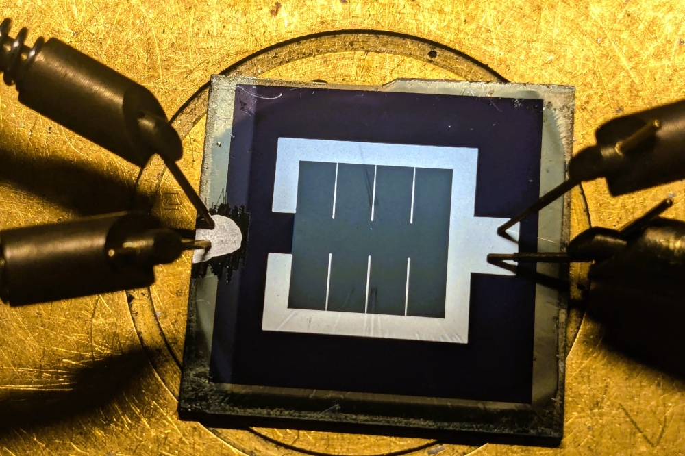
a) Schematic cross section and (b) micrograph of the fabricated vertically oriented trench MOSFET.
Research reported in Applied Physics Express (APEX) by Tohru Oka and colleagues at the Research and Development Headquarters for Toyoda Gosei in Japan describes the development of 'vertically orientated' GaN-based transistors with blocking voltages exceeding 1kV. These findings are important for the application of nitride devices in automobiles and related areas.
Low resistance resulting in reduced power consumption and heating have attracted researchers to study GaN systems for nanoelectronics. Previous work has focused on laterally oriented GaN and AlGaN transistors, which readily provide a high mobility and low resistance. However these structures are limited in terms of the break-down and threshold voltage that can be achieved without compromising device size, which may make them unsuitable for automobile applications. Now Tohru Oka and colleagues at the Research and Development Headquarters for Toyoda Gosei Co, Ltd in Japan have shown how they can overcome these limitations.
Oka and his team adopted the vertical orientation. Previous work has already shown that in this orientation the breakdown voltage can be increased by increasing the drift region thickness without compromising the device size. However, so far these structures have still been limited in the blocking voltage that the device can withstand while maintaining a low on-resistance.
"We redesigned the thicknesses and doping concentrations of channel and drift layers to reduce the resistances of the epitaxial layers while maintaining a blocking voltage of over 1.2kV," explain Oka and colleagues in the report of their work. They also use hexagonally shaped trench gates to increase the gate width per unit area thereby reducing the specific on-resistance. "These led to the excellent performance of 1.2kV-class vertical GaN MOSFETs with a specific on-resistance of less than 2mΩ cm2," they conclude.
'1.8mΩcm2 vertical GaN-based trench metal-oxide-semiconductor field-effect transistors on a free-standing GaN substrate for 1.2-kV-class operation' by Tohru Oka et al; Applied Physics Express 8, 054101 (2015).


