Future electronics: Black phosphorus surges ahead of graphene
Scientists reported a tunable band gap in BP, effectively modifying the semiconducting material into a unique state of matter with anisotropic dispersion. This research outcome potentially allows for great flexibility in the design and optimization of electronic and optoelectronic devices like solar panels and telecommunication lasers.
![]()
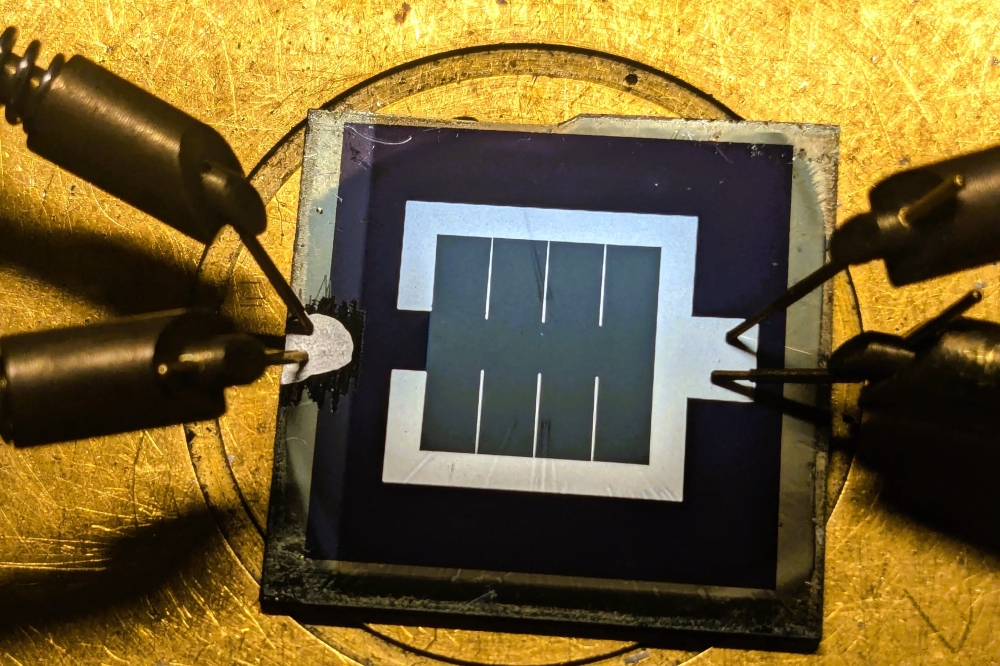
The research team operating out of Pohang University of Science and Technology, affiliated with the Institute for Basic Science's Center for Artificial Low Dimensional Electronic Systems, reported a tunable band gap in BP, effectively modifying the semiconducting material into a unique state of matter with anisotropic dispersion. This research outcome potentially allows for great flexibility in the design and optimization of electronic and optoelectronic devices like solar panels and telecommunication lasers. Credit: Institute for Basic Science
The research team operating out of Pohang University of Science and Technology, affiliated with the Institute for Basic Science's Centre for Artificial Low Dimensional Electronic Systems, reported a tunable band gap in BP, effectively modifying the semiconducting material into a unique state of matter with anisotropic dispersion. This research outcome potentially allows for great flexibility in the design and optimization of electronic and optoelectronic devices like solar panels and telecommunication lasers.
Credit: Institute for Basic Science
A Korean team of scientists tune BP's band gap to form a superior conductor, allowing for the application to be mass produced for electronic and optoelectronics devices.
The research team operating out of Pohang University of Science and Technology (POSTECH), affiliated with the Institute for Basic Science's (IBS) Center for Artificial Low Dimensional Electronic Systems (CALDES), reported a tunable band gap in BP, effectively modifying the semiconducting material into a unique state of matter with anisotropic dispersion. This research outcome potentially allows for great flexibility in the design and optimization of electronic and optoelectronic devices like solar panels and telecommunication lasers.
To truly understand the significance of the team's findings, it's instrumental to understand the nature of two-dimensional (2-D) materials, and for that one must go back to 2010 when the world of 2-D materials was dominated by a simple thin sheet of carbon, a layered form of carbon atoms constructed to resemble honeycomb, called graphene. Graphene was globally heralded as a wonder-material thanks to the work of two British scientists who won the Nobel Prize for Physics for their research on it.
Graphene is extremely thin and has remarkable attributes. It is stronger than steel yet many times lighter, more conductive than copper and more flexible than rubber. All these properties combined make it a tremendous conductor of heat and electricity. A defect-free layer is also impermeable to all atoms and molecules. This amalgamation makes it a terrifically attractive material to apply to scientific developments in a wide variety of fields, such as electronics, aerospace and sports. For all its dazzling promise there is however a disadvantage; graphene has no band gap.
Stpping Stones to a Unique State
A material's band gap is fundamental to determining its electrical conductivity. Imagine two river crossings, one with tightly-packed stepping-stones, and the other with large gaps between stones. The former is far easier to traverse because a jump between two tightly-packed stones requires less energy. A band gap is much the same; the smaller the gap the more efficiently the current can move across the material and the stronger the current.
Graphene has a band gap of zero in its natural state, however, and so acts like a conductor; the semiconductor potential can't be realized because the conductivity can't be shut off, even at low temperatures. This obviously dilutes its appeal as a semiconductor, as shutting off conductivity is a vital part of a semiconductor's function.
Birth of a Revolution
Phosphorus is the fifteenth element in the periodic table and lends its name to an entire class of compounds. Indeed it could be considered an archetype of chemistry itself. Black phosphorus is the stable form of white phosphorus and gets its name from its distinctive color. Like graphene, BP is a semiconductor and also cheap to mass produce. The one big difference between the two is BP's natural band gap, allowing the material to switch its electrical current on and off. The research team tested on few layers of BP called phosphorene which is an allotrope of phosphorus.
Keun Su Kim, an amiable professor stationed at POSTECH speaks in rapid bursts when detailing the experiment, "We transferred electrons from the dopant -- potassium -- to the surface of the black phosphorus, which confined the electrons and allowed us to manipulate this state. Potassium produces a strong electrical field which is what we required to tune the size of the band gap."
This process of transferring electrons is known as doping and induced a giant Stark effect, which tuned the band gap allowing the valence and conductive bands to move closer together, effectively lowering the band gap and drastically altering it to a value between 0.0 ~ 0.6 electron Volt (eV) from its original intrinsic value of 0.35 eV. Professor Kim explained, "Graphene is a Dirac semimetal. It's more efficient in its natural state than black phosphorus but it's difficult to open its band gap; therefore we tuned BP's band gap to resemble the natural state of graphene, a unique state of matter that is different from conventional semiconductors."
The potential for this new improved form of black phosphorus is beyond anything the Korean team hoped for, and very soon it could potentially be applied to several sectors including engineering where electrical engineers can adjust the band gap and create devises with the exact behaviour desired. The 2-D revolution, it seems, has arrived and is here for the long run.


