New S-Grade SiC Devices offer superior performance
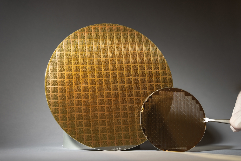
Acme Advanced Materials has announced it has partnered with two of the world's leading SiC research groups to independently evaluate and assess the performance enhancement from devices fabricated on its microgravity processed SiC substrates (S Grade).
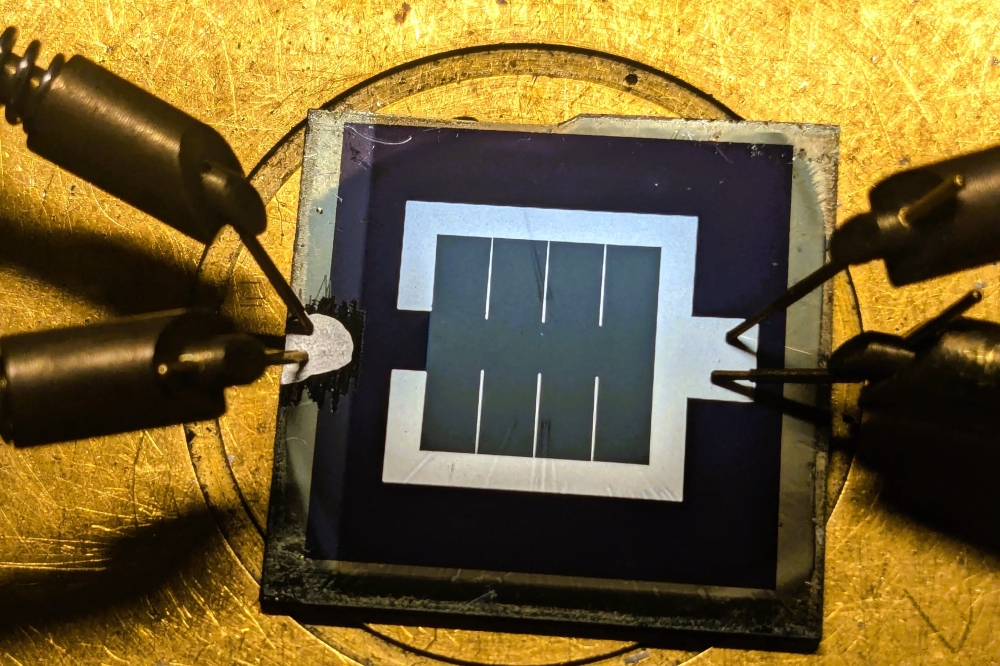
When compared to devices made on traditional Prime Grade substrates, Acme's initial tests showed that the S Grade devices had many benefits including improved electronic transport, lower on-resistance, reduced forward voltage, higher current density threshold and increased reliability.
In order to provide independent verification of these results and develop a deeper understanding of the microgravity process itself, Acme has partnered with Debbie G. Senesky who runs the EXtreme Environment Microsystems Laboratory (XLab) at Stanford University and Michael Dudley, chairman of the Dept. of Materials Science & Engineering at Stony Brook University. Senesky's group has been working with Acme since Jan 2015 to analyse S Grade substrate material properties and build Schottky diode test devices on S Grade substrates. Dudley joined the team in July and his group will bring additional evaluation tools and expertise to the analysis.
"We're really excited about partnering with such well-respected and talented groups to provide new insights and independent analysis of our results," said Acme's president & CEO Rich Glover, "The typical reaction we get from industry when they see our results is, "˜No way, this can't be true.' So, we decided to partner with experts that are well known in the Power Electronics Field and let them perform their own independent analysis."
The initial, first generation device improvements using Acme's grade SiC material will include: faster allowable switching dV/dt for converters, improved short circuit survivability, and superior MOSFET, transistor & diode avalanche energy clamping capability.
"We've conducted detailed preflight and post flight analysis on these substrates and observe compelling modifications to the material structure," said Senesky, "The devices we've built on S Grade substrates also show improved electrical performance when compared to devices built on traditional, unprocessed substrates. My team is digging into these results and we plan to start publishing and sharing the results soon." Senesky added, "These results are quite intriguing and we're looking forward to working with Dudley and applying his unique expertise in SiC microstructure to perform additional analysis."
According to Dudley: "These results are really quite interesting and I'm looking forward to working with Acme and Senesky to evaluate and assess this S Grade material."
ACME Advanced Materials (A2M) was formed to exploit breakthrough technology that was developed and demonstrated by Masterson Industries. The Masterson merger with A2M was completed on January 27, 2014 and A2M is the sole surviving entity. A2M is the parent company to a family of wholly owned subsidiaries with each subsidiary established to further develop and commercialize unique A2M technologies. A2M is a privately owned corporation supported by funding from both US and International venture groups.


