UES develops GaAs-based Photoconductive Semiconductor Switch
![]()
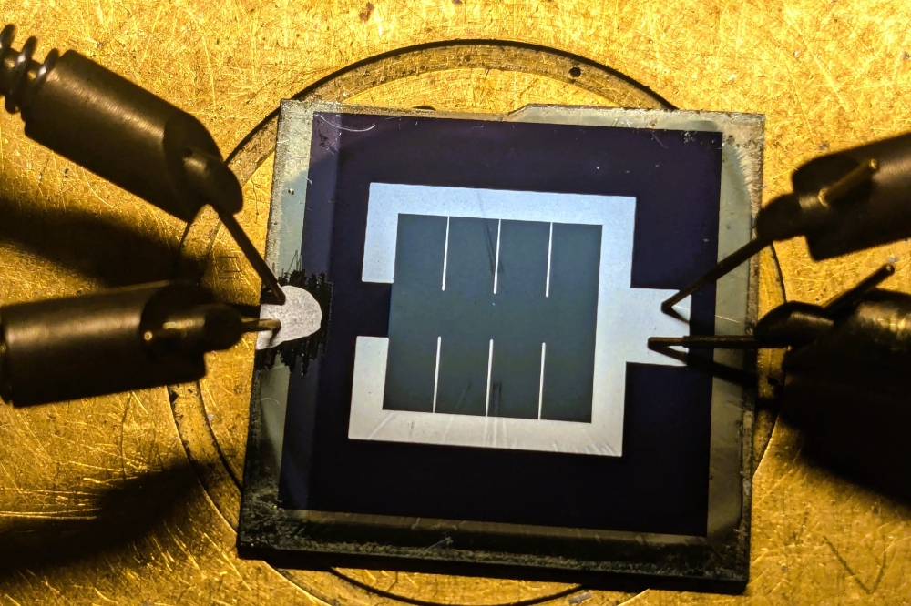
Above (left) Ion bands in PCSS and (right) the PCSS device
In partnership with the US Defense Threat Reduction Agency (DTRA), scientists at UES Inc in Dayton Ohio have developed a durable, high-gain optically triggered photoconductive semiconductor switch (PCSS) based on GaAs. The device, they say, provides unique power handling advantages (voltage hold-off ~ 75kV/cm) and ultralow rise times and jitter (600-800ps).
PCSS devices are turned on by a short laser pulse so they can switch high voltages and high current without requiring a directly connected electrical trigger system. Once the device is turned on, the semiconductor can continue conducting through a stable electron avalanche process.
PCSS Switches with long lifetimes can be used for simulation of nuclear weapon effects and for the active interrogation of special nuclear materials. Lower power PCSS devices can be used in aircraft radars, vehicle collision avoidance systems, and ultra-wideband sensor systems.
Prior work on PCSS technology has shown the need for multichanneling for current conduction to avoid short switch lifetimes. UES has demonstrated multichanneling using an innovative technique of ion irradiation to form parallel conducting channels in GaAs based devices using the high energy Tandetron accelerator. According to UES, this has the effect of eliminating filamentary current breakdown in GaAs PCSSs. In addition, it eliminates the need for bulky laser devices currently used for multichanneling.
The resultant PCSS device handles up to 75kV operating voltage, with a total current of ~ 1kA. Individual channel current has been measured at around 20A/channel at 1kA, with a risetime of 600-800ps. The device is remarkably compact, with functional dimensions of 1 to 2cm on side, and can be triggered with low incident energies of 50-150 microjoules/sq cm. UES in combination with L3 Inc., will now use of the PCSS technology in a modular EMP source.
In this work, the team achieved: a switch capable of handling 75MW power, with a rise time of < 1ns; 80-100 kV operating voltages per module; 1m2 aperture per module (a small footprint compared with point source); and a peak electric field of 70-90 kV/m in test volume.
The EMP generation modules are autonomous and require only external command sequencing and timephased trigger via fibre-optic to each module.
The work will be published via a patent, and has also been selected as a finalist for the 2015 R&D 100 awards.


