III-V/silicon structure shows promise for on-chip lasers

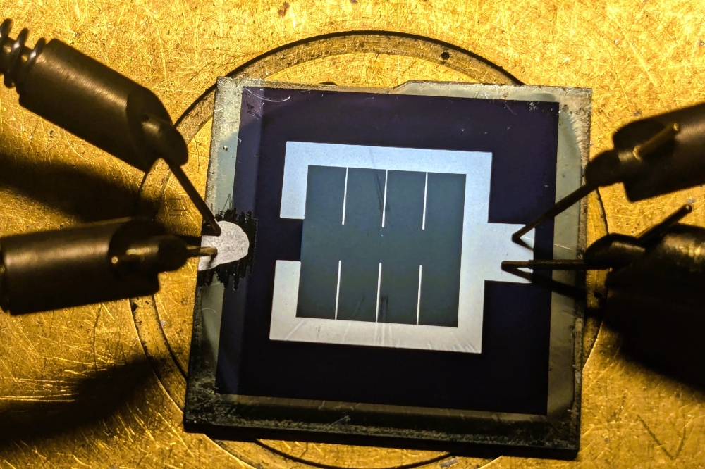
Researchers at Singapore's Agency for Science, Technology and Research (A*STAR) have developed a compact heterogeneously integrated III-V/silicon laser structure that consists of a III-V ridge waveguide gain section on silicon, III-V/silicon optical vertical interconnect accesses (VIAs), and silicon-on-insulator (SOI) nanophotonic waveguide sections.
Compact lasers small enough to be integrated on chip are in great demand for a diverse range of applications, including data communication and storage.
Lasers made from a combination of silicon and III-V structures are particularly attractive as on-chip light sources. But to be useful such lasers must tightly confine light to maximise the lasing efficiency and should effectively share, or 'couple', light with optical waveguides under the laser.
The researchers think their new structure is promising as an on-chip light source for current silicon photonics technology but also as a potential new integration platform. It improves on conventional fabrication procedures, in which components are made separately and then combined, and enables fully integrated optoelectronic systems to be fabricated that take up less space on a chip.
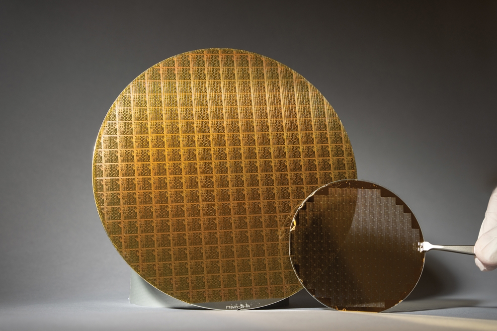
The III-V semiconductor layers are introduced on top of the 300-nm-thick SOI layer through low temperature, plasma-assisted direct wafer-bonding and etched to form a III-V ridge waveguide on silicon as the gain section. The optical VIA is formed by tapering the III-V and the beneath SOI in the same direction with a length of 50µm for efficient coupling of light down to the 600nm wide silicon nanophotonic waveguide or vice versa.
The fabricated Fabry-Perot (FP) laser shows a continuous-wave lasing with a threshold current of 65 mA at room temperature, and the slope efficiency from single facet is 144mW/A. The maximal single facet emitting power is about 4.5mW at a current of 100 mA, and the side-mode suppression ratio is around30dB
This new heterogeneously integrated III-V/Si laser structure demonstrated enables more complex laser configuration with a sub-system on-chip for various applications.
"˜Heterogeneously integrated III-V laser on thin SOI with compact optical vertical interconnect access' by Jing Pu et al; Optics Letters Vol. 40, Issue 7 (2015)


