Cutting grooves in GaAs increases THz emission
![]()
Sitting between infrared and microwave radiation, the terahertz (THz) part of the electromagnetic spectrum has been largely unused due to a lack of cheap ways to mass-produce THz-based devices.
Now research published in Optics Letters by the Femtosecond Spectroscopy Unit at the Okinawa Institute of Science and Technology Graduate University (OIST) in Japan, suggests a solution to the 'terahertz gap' might lie in altering the microstructure of THz emission GaAs-based devices.
THz radiation can penetrate fabrics, paper, cardboard, plastics, wood, and ceramics. Many materials have a unique 'fingerprint' in the THz band allowing their easy identification with THz scanners. Moreover, THz radiation is safe for live tissues and DNA, due to its non-ionising properties. Because of these properties, many believe that being able to exploit THz wavelengths could open up new approaches to medical imaging, detection of chemicals such as explosives, and even data communication.
Today, however, generating THz waves is difficult since the frequency is too high for conventional radio transmitters, but too low for optical transmitters, like the majority of lasers. One of the most frequently used THz emitters is a photoconductive antenna, comprising two electric contacts and a thin film of semiconductor, often GaAs, between them. When the antenna is exposed to a short pulse from a laser, the photons excite electrons in the semiconductor, and a short burst of THz radiation is produced. Thus the energy of the laser beam is transformed into a THz electro-magnetic wave.
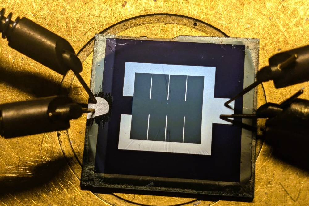
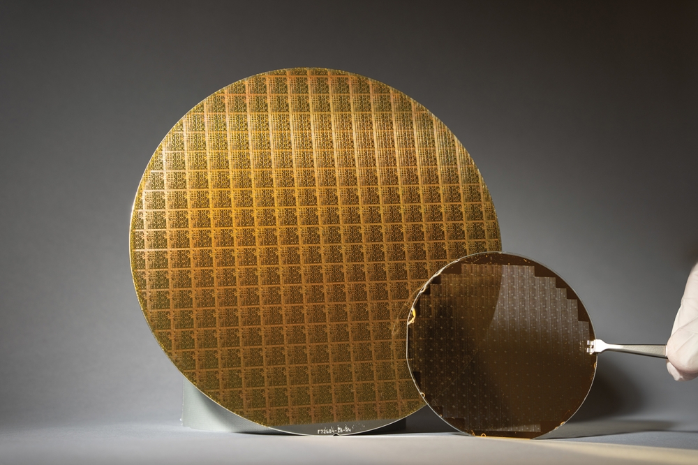
OIST researchers have showed that the micro-structure of the semiconductor surface plays an important role in this process. Femtosecond-laser-ablation, in which the material is exposed to ultrashort bursts of high energy, creates micrometre-scale grooves and ripples (pictured above) on the surface of GaAs. "The light gets trapped in these ripples", says Athanasios Margiolakis, a Special Research Student at OIST. Since more light is absorbed by the ablated material, the efficiency of THz emission, given a sufficiently powerful laser, increases by 65 percent.
Other properties of the material change as well. For example, ablated GaAs shows only a third of the electrical current of non-ablated GaAs. "We observe counter-intuitive phenomena," the researchers write, "One generally expects that the material showing the higher photocurrent would give the best THz emitter." They explain this phenomenon by shorter carrier lifetimes. That is, electrons in ablated samples return to non-agitated states much faster than in control samples.
Julien Madéo, part of the OIST team, says: "Femtosecond-laser ablation allows us to engineer the properties of materials and to overcome their intrinsic limitations, leading, for example, to near 100 percent photon absorption as well as broader absorption bandwidth, control of the electron concentration and lifetime".
The researchers believe that the technique is a fast, lower-cost alternative to existing methods of manufacturing materials for THz applications.
'Ultrafast properties of femtosecond-laser-ablated GaAs and its application to terahertz optoelectronics', by Julien Madéo et al; Optics Letters, Vol. 40, issue 14 (2015)


