MIT and NRF SIngapore enter fourth year of optical chip development
![]()
The Singapore-Massachusetts Institute of Technology (MIT) Alliance for Research and Technology (SMART) has announced entering its eighth year of investigating new technologies. As part of this, MIT's Eugene Fitzgerald and the National Research Foundation of Singapore (NRF) are now working on their fourth year of developing optical chips from III-V and silicon as part of the SMART LEES program.
"With integrating III-V and other materials with silicon technology, we are designing circuits that nobody could conceive of, such as building lighting systems on a chip," Fitzgerald (pictured above) explains.
"We're making the silicon fab the entire supply chain for the lighting system, so you get a complete programmable lighting surface, including driver circuitry and intelligence in a very small footprint. Ideally, you could drop III-V devices into circuits whenever you want to communicate with the outside world, by wireless or optical communication."
The monolithic integration of LEDs with silicon electronics could greatly reduce the cost of smart LED lighting, and potentially lead to thin displays with their own optical inter-device communications via light pulses. The result might be a more secure alternative to WiFi, he adds.
"Once the display and computer merge into a single device, you can define new capabilities," says Fitzgerald. "For example, a very thin display with multiple functionality in a single device is possible. This opens up possibilities such as a smartwatch display that is also a solar cell that charges the device. You could even reprogram the same display to act as a scanner."
Initially, the technology will be used for a variety of task-specific devices with similar hardware. "But once volume ramps up you could have common platforms where all these capabilities reside," Fitzgerald says. "It would be like a tricorder where you can program it to do a lot of different things."
SMART LEES is also experimenting with a business model that makes it easier for novel integrated circuits to reach market. "Today we have huge fabs that ship huge amounts of wafers," Fitzgerald says. "The problem is that whenever someone comes up with a new device or material, it's difficult to insert it into the manufacturing infrastructure. They're making sugar cookies and you're telling them you want chocolate chip cookies - and they don't want chocolate chips anywhere near their facilities."
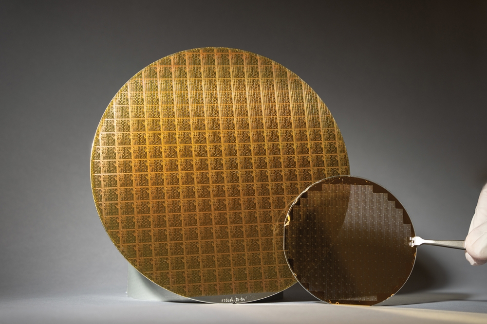
The SMART LEES solution is to use a standard design kit to build upon a standard wafer made in a real fab, but then stop the manufacturing process in the middle. "At that point, we bring the wafer back to R&D to add new materials or devices in a way that can be compatible with the fab," Fitzgerald explains. "The device can then be finished using the standard processes. This way, you can produce new ICs for smaller markets without having to build a new process or a $5 billion plant for every new product."
The combination of the integrating new materials and devices with silicon, combined with new approaches to fabrication, could lead to the same sort of long-lasting benefits as Moore's Law, says Fitzgerald. He notes, however, that "the next paradigm usually comes from where you least expect it."


