
Lasertec launches SiC wafer inspection and review system
Lasertec has launched SICA88, the latest model of its SiC wafer inspection and review systems. Featuring both surface and photoluminescence (PL) inspection capabilities, SICA88 enables customers to concurrently inspect and analyse surface defects as well as crystallographic defects, according to the company.
Lasertec has already started sales promotion of SICA 88 and received orders from multiple customers including Rohm.
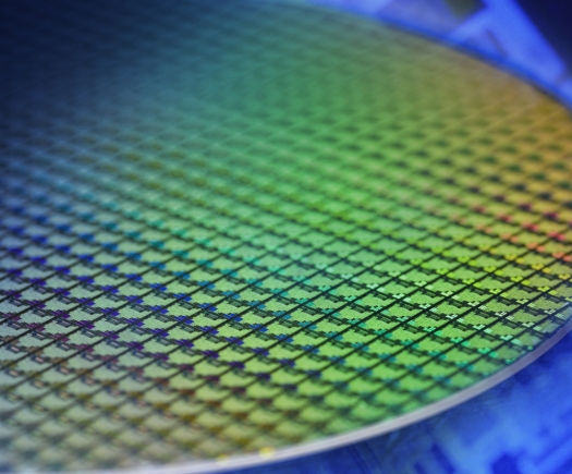
While SiC power devices are already being used in air conditioners, solar cells, trains and other power applications, producing them is technically demanding. Various problems remain unsolved, including crystallographic defects that occur in production process. Quality control and cost reduction pose major challenges. SiC wafer manufacturers find it necessary to enhance and maintain wafer quality while SiC device manufacturers are expected to keep higher yields and reduce production cost.
SICA is an inspection tool that is designed to help overcome these challenges. Lasertec launched SICA61 in 2009 for R&D use and SICA6X in 2011 for production use. Since then, SICA has become renowned for its high sensitivity and accurate defect classification capability and widely adopted by many customers.
SICA88 introduces a new platform that combines the PL inspection capability with the confocal DIC optics used in the previous generation SICA models for surface inspection.
It now offers simultaneous detection and classification of not only scratches and epitaxial defects on the wafer surface but also crystallographic defects such as basal plane dislocations (BPD) and stacking faults (SF) inside epi layers, thereby assisting the detection and analysis of defects that cause device malfunctions. The throughput of SICA88 is twice as high as that of SICA6X and, furthermore, BPD inspection is possible without compromising the throughput performance.
Lasertec says that one of the best ways to use SICA88 is as a process monitor in wafer production, epi process and device making process for assisting root cause analysis. It also offers a wafer grading capability that helps achieve process cost reductions and higher device yields.


