Panasonic Develops high current, low turn-on GaN Diodes
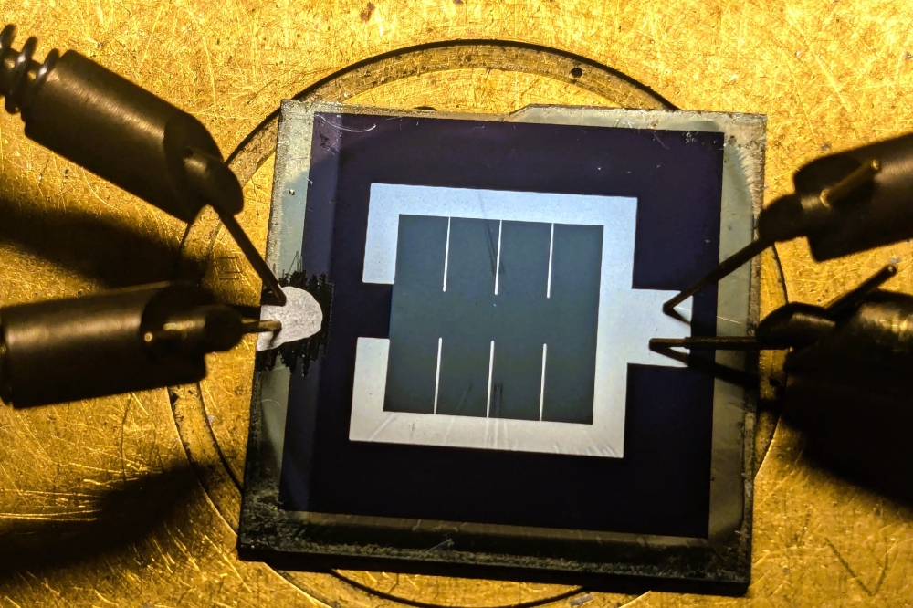
Panasonic has developed GaN diodes that can not only operate at current four times greater than tolerated by conventional SiC diodes (with a rated voltage of 1200V), but also at a low voltage by virtue of their low turn-on voltage.
The new diodes are built using a newly developed hybrid structure composed of a separately embedded low-voltage unit and a high-current-capable unit, in preparation for high voltage conditions.
Conventional silicon diodes are limited with regard to reducing switching losses. On the other hand, SiC and GaN need greater chip area to achieve high-current operation, posing limitations on the reduction of switching losses and size owing to increased operating frequencies.
These new GaN diodes have achieved simultaneous high-current operations and low threshold voltage to handle high currents even with a small chip area, according to the company. The capacitance of the chip can therefore be reduced to achieve lower switching losses, allowing the device to operate at higher frequencies. As a result, use of GaN diodes in the voltage conversion circuits or inverter circuits of automotive or industrial equipment that requires high power can reduce system size due to high frequency operation.
High-current operation is 7.6 kA/cm2, turn-on voltage is 0.8V, on-resistance is 1.3 mΩcm2 (approximately 50 percent reduction)
The hybrid GaN diodes are based on a trenched p-GaN layer. Panasonic has developed a processing technology that can remove a p-type layer on an n-type layer in a selective manner to achieve not only high-current operations and a low turn-on voltage but also a breakdown voltage of 1.6 kV.
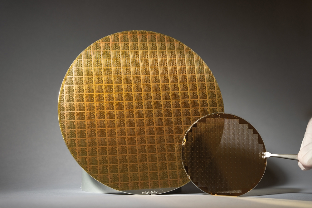
The company used conductive GaN substrates (these are commercially used in LEDs and semiconductor lasers and are expected to be adopted in power devices in the future), and established the technologies for the epitaxial growth and processing on a GaN substrate before forming diodes. A structure in which currents flow in the vertical direction enables a smaller chip area and lower resistance.
Results were presented at the 2015 International Conference on Solid State Devices and Materials , Sapporo, Japan (September, 2015)
The work was partially supported by the Ministry of the Environment, Government of Japan.


