Plessey's dotLEDs nominated for Elektra award
Chip scale LEDs for wearables shortlisted for Design Team of The Year
![]()
Plessey has announced that its chip scale packaged dotLEDs have been shortlisted in Elektra Awards' category of Design Team of The Year. Acknowledging product innovation and business success in the industry for more than a decade, the Elektra Awards celebrates the achievements of individuals and companies across the electronics industry. The awards showcase the finest new products, technology innovation and company performances of the year.
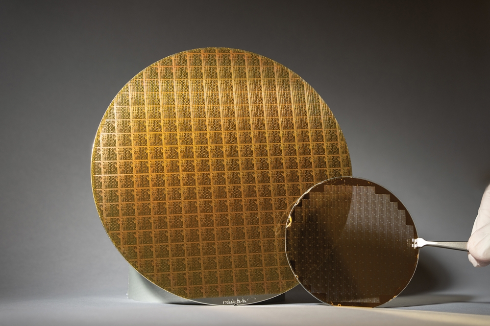
The CSP-300's core LED chip is based on Plessey's proprietary GaN-on-Silicon manufacturing technology, which is built on six-inch silicon wafers. This technology enables the lowest LED product cost combined with a superior thermal performance compared to competing technologies. Designed for wearable technology applications such as smart watches, mobile backlighting and textiles, the dotLED has a footprint of only 0.55mm x 0.55mm and offers multiple whites, red, green and blue colours with various levels of light output.
Zainul Fiteri, Plessey's LED Packaging Specialist, said: "Demand for wearable technology is increasing and LED technology plays an increasingly major role in product realisation in this sector. The CSP-300 is designed to deliver the best, smallest size, lowest cost LED solution and therefore fulfil the needs of this emerging market.
"The manufacturing process uses wafer level packaging with Through Silicon Via (TSV) technology - a greatly simplified process compared to conventional LED packaging technologies with a shorter manufacturing cycle time, very high throughput and hence reduced cost. The unique combination of the six-inch, silicon LED growth wafer process and the eight-inch, silicon packaging wafer process results in significant economies of scale in manufacturing.
"The dotLED is the smallest wearable LED in the market with a true optical centre in a square form factor. This feature has critical impact in the end application, for example when it is desired to build a miniature array of devices in a display application. Competitive products with non-optimal centring and larger footprints do not allow the same small form factor arrays to be manufactured. With our design and manufacturing technology, and future evolution of circuit assembly techniques, future products could be as small as a 0.27mm square footprint with the same performance."
Selected by an independent panel of judges, the winners will be announced on Tuesday 24th November 2015 at the awards ceremony taking place at The Lancaster Hotel in London. Other companies shortlisted for within the category Design Team of The Year are ByteSnap Design, ESCATEC, AndersDX and Peratech.


