
Plessey: bright and bold
With a hefty £30m bank loan and massive expansion underway, where next for GaN-on-silicon LED pioneer, Plessey, asks Compound Semiconductor.
Plessey's expansion plans include maintaining manufacturing in the UK, at least for the next three years.
Late last month, UK-based Plessey revealed plans for a massive £60 million expansion at its Plymouth LED facility, after securing a £30m loan from Deutsch Bank and having won £6.7m in local government funds.
"To actually get a tier one bank on board at this stage [of our company development] is quite an achievement and very exciting for us," Plessey's chief financial officer, Iain Silvester, tells Compound Semiconductor.
"Using the Deutsch Bank Loan, Regional Growth Funds and our own cash generation, we will now add capacity as sales ramp," he adds.
Expansion plans are aggressive. Over the next two and a half to three years, the company intends to increase production capabilities by a factor of thirty - adding at least ten new reactors to the facility - while more than tripling the workforce to around 535 employees.
According to Silvester, come the end of next year around 150 new employees will already be on board, doubling today's headcount. The lion-share of new jobs will fall within the facility itself, with Plessey hiring more MOCVD operators, process engineers and skilled workers to manage the facility.
"We will see fairly modest growth on the commercial side of the business, but we operate all day and night, so really, this is going to be about scaling up production," says Silvester.
 By the end of next year, Plessey intends to have doubled its number of employees.
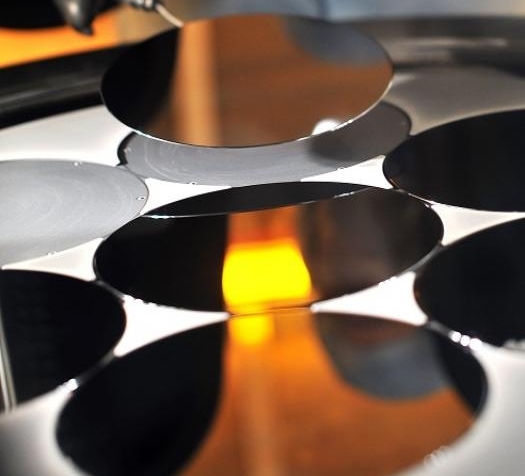
Since 2010, Plessey has been developing GaN-on-silicon LEDs using two Aixtron Crius II MOCVD reactors in a 7X6-inch wafer configuration. But this is set to change.
As Mike Snaith, Plessey's operations director points out, the company has all the necessary tools to support current MOCVD throughput, with some redundancy.
However, to scale production, Plessey will now buy two additional reactors and expand bulk gas capability ready for at least another ten MOCVD reactor chambers, capable of six-inch and eight-inch LED manufacture. The company has yet to confirm whether or not the new reactors will be sourced from Aixtron, Germany, or Veeco, US.
"Our Plymouth site has three clean room areas and our intention is to have all in-house capability for high volume MOCVD GaN on Silicon growth, high precision and large die alignment, deep trench etch, wafer bond and lift-off as well as a full back-end toolset," says Snaith. "One of the clean rooms will retain CMOS tooling to add additional passive components and allow for the manufacture of monolithic LEDs."
And production will, at least for now, remain at Plymouth. "A typical competitor will have between fifty and one hundred reactors, and we are now looking to have about fifteen in our facility over the next three to four years," says Silvester.
"Whether or not we continue to manufacture in the UK, beyond this point, we will have to see, but growth over the next four years will certainly be driven by our Plymouth facility," he adds.
More integration
In addition to rapid expansion, silicon-based chip-scale packaging is well underway at Plessey, and the company intends to develop a range of integrated LED devices, that have, for example, power management and sensors, integrated into the silicon platform.
At the same time, the company has recently patented technology relating to chip-scale optics, in which the LED lens is integrated on-chip. According to Silvester, development will now continue apace, with the first integrated LED products reaching market as early as the second quarter of next year.
"Everyone understands the cost advantage that using silicon wafers will bring but this is actually secondary to some of the integration that we can provide within the device," says Silvester. "Silicon substrates offer opportunities that just aren't available to sapphire, so using our existing CMOS skills and our engineering base, we will now develop these integrated LED devices."
But integration aside, a key goal for Plessey has been to move from six inch to eight inch wafer fabrication.
The LED manufacturer has been working closely with Aixtron to address the MOCVD reactor re-tooling issues that accompany scaling, and Silvester asserts the latest Deutsche Bank backing will now accelerate this transition.
"We have an ongoing programme devoted to our eight inch process and most certainly we'll be moving towards eight inch production within four years," he says.
"Next year the new reactors will be six inch and beyond that we'll be re-tooling to eight inch," he adds. "Clearly a key goal is to set up eight inch production as fast as we can."


