Delivering the future

With III-V and CMOS integration well underway, novel ICs from Singapore-MIT program, SMART-LEES, could reach market soon. Compound Semiconductor reports.
The goal for the SMART-LEES program is to develop fundamentally new ICs; its researchers are getting close.
From the outset, researchers from the Singapore-MIT Alliance for Research and Technology, working on low energy electronics systems, decided not to reinvent the wheel.
Brought together by the Singapore government and MIT in January 2012, the SMART-LEES team intends to create fundamentally new integrated circuits based on III-V materials and silicon as Moore's Law collapses.
And according to Professor Eugene Fitzgerald, MIT, working with silicon has always been the priority.
"Silicon foundries already have CMOS manufacturing in place and these organisations can't be expected to change processes just to carry out crazy stuff for universities," he says.
"Yet, whenever someone comes up with a new device it is difficult to insert that into the manufacturing infrastructure."
"We know from a capital point of view it doesn't make sense to build new infrastructure end to end for this," he adds. "So from the very beginning we have said that III-V materials have to fit into a silicon design kit."
With this in mind, researchers from the SMART-LEES program, based at MIT, National University of Singapore and Nanyang Technological University, have been working with myriad industrial partners on this very issue.
Silicon CMOS powerhouses, Global Foundries, Singapore, and Japan-based Tower Semiconductor-Panasonic joint venture, TPSCo, are key manufacturing partners.
Meanwhile Aixtron, Germany, IQE, UK, Austria-based EVG, and Samco of Japan, all join forces with the project later on along the IC supply chain.
And with weighty board members from IQE, Netherlands-based Lumileds and Analog Devices, US, also backing the the project, SMART-LEES clearly has clout.
"We set up the board to have stakeholders that would be interested in seeing this succeed," highlights Fitzgerald.
"But we also put together a research team from materials, device and circuit design that can simultaneously influence each other," he adds. "And because we can't re-work the entire CMOS process, we developed 'modular processing'."
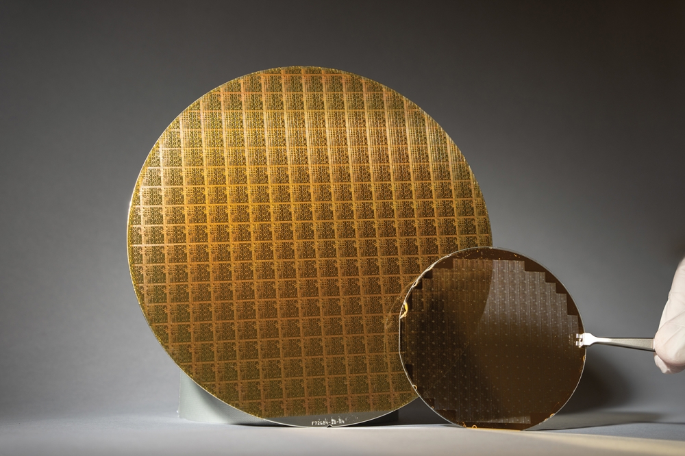
Here, the researchers take 200 mm silicon wafers from the front-end of their partners CMOS manufacturing processes and then use existing CMOS design tools to develop novel ICs at the SMART-LEES 200m facility in Singapore.
This fab houses two AIXTRON CRIUS reactors and in-situ optical monitoring tools, so here, III-V layers are added and devices are fabricated.
The wafer is then returned to the foundry for the back-end processes that connect the III-V and silicon CMOS devices within the die.
"We've set up LEES so we can add any kind of III-V material, but it has to be done so that the wafer looks like it never left the foundry," says Fitzgerald. "The wafer will return with dielectric and contact areas so that you start the back-end of the foundry process, it looks like it never left."
And as he adds: "What this actually does is to induce innovation that is exactly aligned to future manufacturing requirements. We innovate around, say, particular temperatures and processes so [our results] are ready for commercialisation."
Rapid progress
In 2012, the LEES team started work on GaN, GaAs and InP deposition on silicon substrates, but as Fitzgerald points out, 'things have moved on'. The researchers are now focusing on InGaAs and GaN, integrating an InGaAs HEMT, GaN HEMT and GaN LED into silicon design platforms.
"We now have an entire process and design toolkit which can include lattice-mismatch engineering such as aspect ratio trapping and metamorphic buffers," explains the MIT Professor. "We do a lot of epi- and wafer-bonding, and have basically created an engineered substrate that can support whatever device we want."
"We transfer the CMOS processes to the top of this, process the III-V devices... and send them back to the foundry," he adds. "So we can design, for the first time, circuits as part of a very real foundry process, and that's not easy to do. There's no special research process and this is unique."
Clearly, the main thrust of the LEES manufacturing model is to get novel integrated circuits into the market-place faster and more easily, but when will industry see real devices? It could be sooner rather than later.
According to Fitzgerald, test chips will be delivered next year and he expects to see prototypes in very real applications some two to three years later.
"We pretty much know how to put III-Vs onto silicon wafers, but when we started, the complete unknown was how to then transfer the CMOS onto this engineered substrate," he says. "But we're now moving wafers back and forth between the foundry and thanks to sizable enough funding, our companies and researchers can collaborate in ways that wouldn't normally be possible."
"Soon, we're going to have the one thing that everyone wants," he concludes. "And that's to have a design kit for both III-V devices and CMOS."


