Vertical GaN: The Pathway To Power Switching Efficiency

More efficient power switching devices are required to meet the energy demands forecasted over the next 20 years.
BY BRYAN BOTHWELL, DAVID DRUMMOND AND MANYAM PILLA FROM QORVO, AND HUILI GRACE XING AND DEBDEEP JENA FROM CORNELL UNIVERSITYPower semiconductor devices are critical for the world's energy infrastructure as it is projected that by 2030, as much as 80 percent of the electricity generated will pass through one or more power conversion stages from generation to consumption (an increase from 30 percent today). That will propel switching devices, which are already playing a critical role, to even greater prominence.
Modern high-efficiency switching power conversion solutions were enabled by the development of silicon-based power MOSFET switching devices. Power switch device switching and on-resistance (Ron) are two key characteristics that impact the maximum conversion efficiency; their impact is magnified at higher voltage and current levels.
It is here that the drum beats the loudest for higher efficiency, lower-loss switching devices that can service markets ranging from motor drives to electric vehicles and power generation and transmission. These markets are not only looking for greater performance "“ they are also very cost conscious.
Significant improvements in efficiency will not result from further refinements to silicon devices as their performance is already approaching the material limits. Instead, industry is turning to the superior material properties of wide bandgap (WBG) GaN and SiC devices to meet the requirements of tomorrow's high-efficiency, low-loss systems.
Devices using SiC and GaN have been commercially available for several years, but widespread adoption has been hampered by high cost and unproven reliability compared to silicon incumbents. But in terms of potential performance, the WBG materials are vastly superior (see, for example, Figure 1).
GaN has superior dielectric strength and electron mobility resulting in an improved figure of merit (FOM) compared to SiC for most power conversion applications; except at extremely high temperatures where SiC trumps all other materials. Assessment of the potential of both materials can be made with various figures of merit "“ the most well-known is that by Baliga, which considers the specific on-resistance of the drift region of the vertical FET. Two other key metrics are the bipolar switching speed and bipolar power handling capacity as seen in Figure 2.
It is possible to achieve cost parity with silicon devices by producing lateral GaN HEMTs with GaN-on-silicon epiwafers, although operating voltages are typically limited to 650 V or less. For higher voltage applications, switching from silicon to SiC substrates overcomes this limitation, but device cost increases due to substrate costs and the increase in lateral device size needed to support the higher voltages.
Figure 1. The ideal material for making power switches must combine a high breakdown voltage with a low on-resistance. Silicon is the most common material for making devices, but many groups have demonstrated wide bandgap devices that exceed the limit of what is capable with that incumbent technology. From both an experimental and a theoretical standpoint, GaN is superior to SiC by a notable margin.
A better approach is to turn to a superior device architecture: A vertical device. Similar to a super-junction MOSFET, a vertical device would meet both the performance and cost requirement by significantly reducing the die size, but requires a homoepitaxial GaN substrate to support the vertical current flow.
The challenge has been to create a vertical power switch device in GaN "“ when solved, this will unlock the door to new levels of cost effective conversion efficiency.
This vision of a new generation of vertical GaN device that increases energy efficiency and trims carbon footprints is held by the US agency ARPA-E. And to turn this dream into a reality, it has funded a three-year, $27 million programme called SWITCHES - Strategies for Wide-Bandgap, Inexpensive Transistors for Controlling High-Efficiency Systems. SWITCHES aims to realize transformational advances in WBG materials, device structures, and fabrication; producing single-die power devices capable of handling voltages in excess of 1200 V and currents of more than 100 A. Fourteen SWITCHES projects were funded.
From lateral to verticalAt the heart of the GaN-on-GaN benefit is the fact that it enables the vertical device. This is superior to lateral devices, where current flows close to the surface in a two-dimensional electron gas (2DEG) layer formed at the AlGaN/GaN interface (see Figure 3). Drawbacks of the lateral geometry are the need for large lateral dimensions proportional to the voltage and current ratings, poor thermal handling capability due to the silicon substrate, and significant current collapse (a reduction in drain current following a switch transition, caused by a memory-like effect of trapped charges on the conduction current in the 2DEG channel). Combined, these factors hinder the cost-effective scaling of lateral devices to high voltage/current ratings.
Figure 2. The great opportunities for wide bandgap devices, and those made from GaN in particular, are evident from the superior figures of merit compared to those based on silicon and GaAs.
A team from the University of California, Santa Barbara, has pioneered the vertical, homoepitaxial GaN devices that address these weaknesses. In such devices, which involve vertical current flow through the GaN substrate, most of the voltage drop takes place in the vertical direction. Consequently, the lateral dimensions do not need to scale with voltage. Thanks to this, die size can be five-or-more-times-smaller than a lateral device. What's more, the vertical architecture virtually eliminates current collapse, while enhancing switching speeds and thermal handling capabilities. However, it is only fair to point out that the vertical device has its challenges: It requires a bipolar junction to realize diode and transistor devices; and due to known material constraints, it is tough to realise impurity-doped p-type GaN.
To address these technological gaps, polarization-doped p-type and n-type layers and associated junctions have been developed by Huili Grace Xing and Debdeep Jena, leaders of a group that has recently relocated from the University of Notre Dame (UND) to Cornell University. Thanks to this breakthrough in doping, it is now possible to form structures with high breakdown voltage, high inversion channel mobility and a low on-resistance. Another key technology is the use of low-cost silicon implantation in the polarization-doped p-region to create an n-channel (see Figure 4).
In addition to the challenges already outlined, if vertical GaN devices are to become a commercial success, they must also overcome issues related to maturity and the supply chain. This class of GaN device has a promising future in motor drives, solar inverters, electric-vehicle charging, telecom DC-to-DC conversion, and within the military "“ but success hinges on a multitude of factors. Of these, performance is paramount, as there is a need for vertical GaN devices delivering higher-efficiency switching while operating at higher frequencies and temperatures. If they can do this, there will be a trimming of size and a cutting of cost at the system level, while critical reliability requirements set by industry are fulfilled.
Those of us from Qorvo are subcontractors on two SWITCHES projects: The first project is led by Huili Grace Xing and Debdeep Jena, and includes IQE and the United Technologies Research Center (see Figure 5 for details); and the second project is led by Microlink, a company specializing in epitaxial lift-off technology that could prove critical in cutting device cost through the re-use of bulk GaN substrates. The small sizes and high costs of GaN substrates have led many leaders in industry and academia to pay minimal attention to GaN-on-GaN devices formed using bulk substrates, but the efforts of Microlink could address this.
Progress to date has been impressive with UND/Cornell having successfully designed and fabricated GaN-on-GaN polar p-n diodes using IQE SWITCHES epi with blocking voltages of more than 1200 V as well as p-n diodes with blocking voltages in excess of 3000 V. These fabricated polarization-induced GaN-on-GaN p-n diodes show near perfect I-V behavior and avalanche capability. PolarMOSH devices have been demonstrated with a threshold voltage of 1.3 V, a maximum on current of 250 mA/mm and a maximum gate voltage of more than 15 V. Beyond this, Qorvo has recently shown blocking voltages of more than 700 V on MBE-regrown JFETs, with plans for a transition to a 4-inch platform in 2015 to address manufacturing maturity and further cost reduction. Key SWITCHES programme milestones continue to be achieved, leading to increased confidence in this technology core.
Figure 4. The PolarMOS technology combines p-n junction devices with MOSH and JFET technologies.
There are still many challenges ahead. One immediate goal is to build on recent successes in substrate and epiwafer improvements, and to demonstrate vertical polar JFETs that can handle 300 V and 10 A. This effort will involve various risk reduction plans at the wafer processing level − mainly targeted at processing control and calibration.
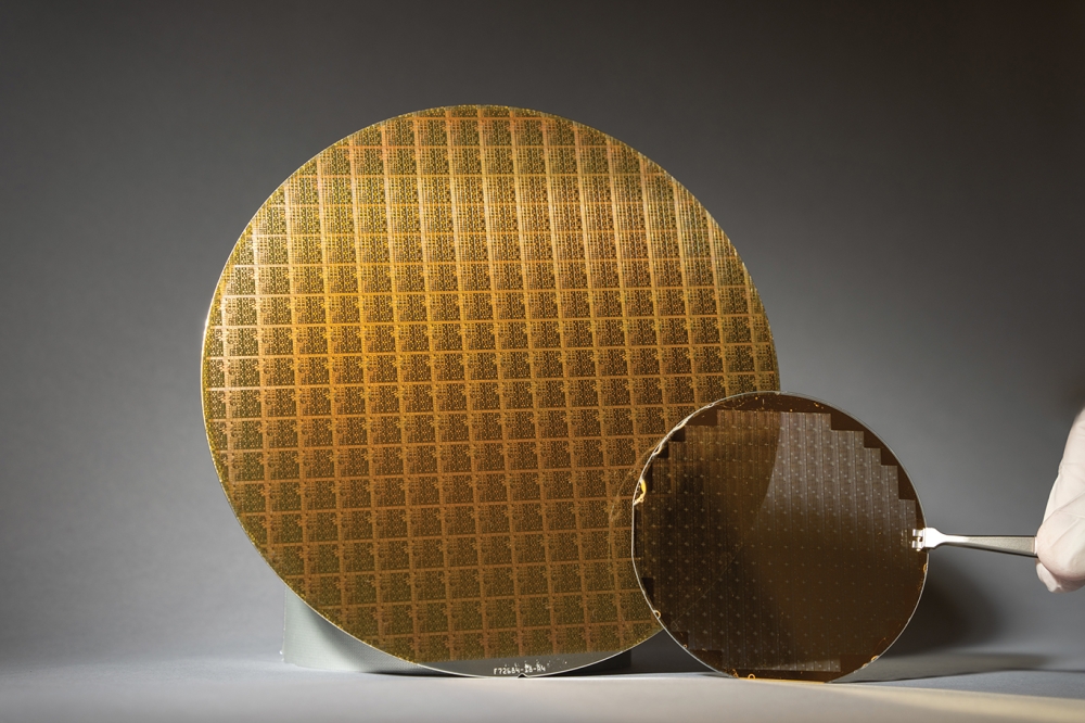
Another challenge is to fabricate large JFETs, capable of operating at 10 A or more, on large-diameter bulk GaN wafers in a 4-inch fab. An aggressive plan is in place to push substrate vendors to 4-inch wafer diameters, which will enable us to accelerate process development and maturation at Qorvo's 4-inch/6-inch fab.
Our next major task is to integrate the polarMOSH and polarJFET processes, and to fabricate polar vertical MOSHFETs − PolarMOS. Although we have demonstrated as-grown material with a blocking voltage in excess of 1200 V, this needs to be repeated with regrown or implanted channels. The good news is that we have developed new technology and intellectual property that enables higher blocking voltages, and combines sufficient margin with improved reliability. Beyond this, integrating the epitaxial lift-off with the new device architecture is planned.
The final challenge will be at the system level to develop packaging solutions for high-power devices in a small form-factor, along with component integration. Qorvo is working with members of both projects to develop packaging solutions that maximize the performance of vertical GaN-on-GaN devices at the system level.
The appeal of these devices is intensifying, thanks to their capability to fulfil the need for low-cost, high-efficiency switching that can trim electricity consumption and accelerate alternative-energy deployments on a global scale.
This places those of us at Qorvo in an enviable position, thanks to our involvement in: a differentiated core device technology; a world-class supply chain and system partners; a high-volume manufacturing infrastructure; and parallel paths, including substrate re-use that addresses cost parity. By developing go-to-market solutions, often a stumbling block for ubiquitous deployment of WBG power devices, an exciting future is on the horizon in power conversion.
Figure 5. The SWITCHES team led by Huili Grace Xing and Debdeep Jena − who have both recently moved their groups from the University of Notre Dame to Cornell University − is very strong and highly complimentary. Xing and Jena are the inventors of the background IP for a differentiated device architecture that addresses the doping issues problematic with vertical GaN devices; IQE is a major epiwafer supplier to the III-V semiconductor industry and possesses not only a world-class engineering background, but also a commercial cost structure needed for a long-term production ramp; UTRC is the research arm of UTC and acts as the technology incubator for their business units who have rich experience in designing power systems for aerospace, defence and commercial applications; and Qorvo is the world's leading supplier of RF devices into the mobile, infrastructure, and defense markets with over 15 years of GaN manufacturing and product development experience. UTRC provides not only a commercial outlet for products from the SWITCHES programme, but more importantly is the partner that helps define product performance, specifications, and overall system level requirements.


