WIN Semiconductors: base stations and beyond

WIN Semiconductor's GaN on SiC process has been optimised for 4G macro-cell base station power amplifiers.
Earlier this month, Taiwan-based WIN Semiconductors unveiled its latest GaN on SiC process for the design and production of power amplifiers, low-noise amplifiers and RF switches.
The 0.45µm-gate MMIC process has been optimised for 4G macro-cell base station power amplifiers operating at 2.7GHz and beyond, and for WIN, this is just the beginning.
The WIN NP45 process will also support 4.5G technologies and next year the company intends to deliver a 0.15µm-gate MMIC technology for devices operating up to 40 GHz, targeting high bandwidth 5G networks and Ka-band applications.
"In the past year, we've seen a significant increase in demand from companies that wish to convert from silicon LDMOS to GaN processes for 4G base station applications," highlights Walter Wohlmuth, associate vice president of technology at WIN Semiconductors.
"Customers tell us the market is here now so we've been optimising the process and layout to meet product specifications and packaging constraints," he adds.
Over the past year, the foundry has been sampling devices and running prototype customer mask sets as customers qualify products for production.
Wohlmuth reckons volume production will start at the end of the second quarter, next year, and at this point, WIN will be able churn out hundreds of wafers a month.
"We have put production capacity in place for 500 wafers a month," he says. "And any company that's currently producing LDMOS [devices] for base stations will be a potential customer as well as companies with compound semiconductor wireless expertise that are eager to enter the base station market."
Wafer sizes
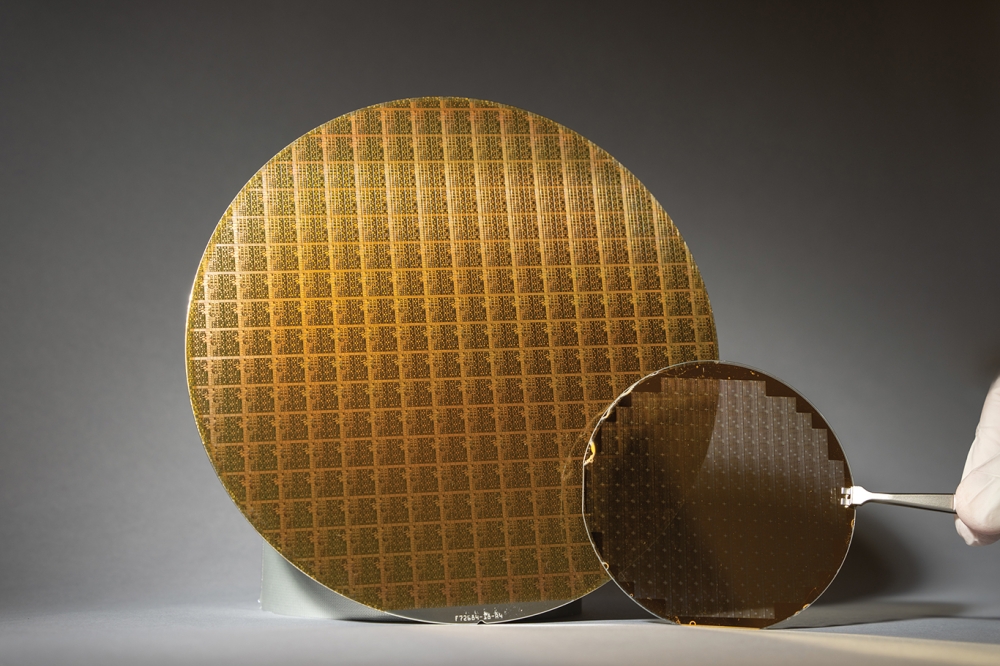
WIN's NP45 technology is currently fabricated on 100mm SiC substrates, and operates at a drain bias of 50V. But why the smaller wafer size?
As Wohlmuth says: "The majority of GaN device fabs working with silicon carbide still seem to be at 100 mm, and we haven't seen significant volumes justifying the move to 150 mm substrates yet."
Still, converting to a 150 mm process is factored into future company plans. "Just like the GaN-on-silicon power switch market, this GaN-on-SiC base station market production volume ramp has been delayed in the past," he says.
"But we are now seeing volumes ramping up in the industry and at a certain volume production level we will convert from 100 mm to 150 mm substrates, which we anticipate will take place within the next two years," he adds.
In the meantime, the company is out to prove its new process. As Wohlmuth points out, the GaN-on-SiC processes from rival players, including Qorvo and Cree, are already fully-operational.
However, WIN's NP25 process has been released for production for almost two years, and the company has transferred significant knowledge and experience from its GaAs processes to its latest GaN technologies.
"For example, we partnered with several equipment companies to re-engineer and optimise the back-side process, leveraged relationships with epi-wafer supply vendors and have shared equipment, facilities, quality, reliability and logistics with the high volume GaAs production staff at WIN," says Wohlmuth.
And as Wohlmuth highlights: "While competitors mostly use more dated equipment that can be difficult to control in production, we've invested in newer equipment and delivered a robust, high volume, high yield production process that can be quickly scaled for increasing production volume."
A future with silicon
But while the foundry is currently firmly focused on the GaN-on-SiC processes, future opportunities may also lie in GaN-on-silicon devices.
In the past, the silicon substrate has been slated for its poor thermal conductivity, relative to SiC. Indeed, telecoms operators have reportedly avoided GaN-on-silicon power amplifiers due to concerns over inadequate heat dissipation leading to field failures.
But this could be changing. As Wohlmuth highlights, the technology is constantly improving and maturing, and of course, silicon substrates have clear cost benefits over the silicon carbide alternative.
"Over time, the high volume base station market could move from discrete transistors to MMICs," he says. "And at this point, the devices will be much larger giving GaN-on-silicon technologies a huge cost advantage."
"Once we have solidified our credibility in the GaN-on-SiC device market, and given our huge GaAs experience, it may be only a matter of time before we develop a GaN-on-silicon process," he adds.


