Transistor reduces power dissipation over 90 percent
![]()
Kaustav Banerjee (right) with researchers in his Nanoelectronics Research Lab at UC Santa Barbara.
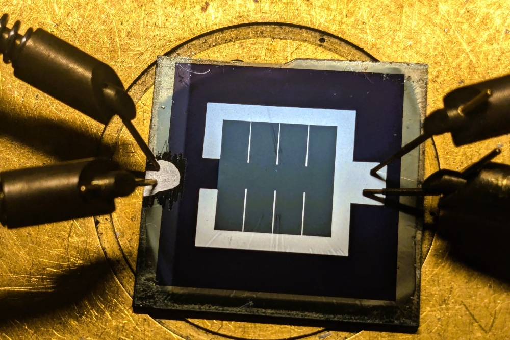
In a study recently reported in Nature, engineers at University of California, Santa Barbara, in collaboration with Rice University, have demonstrated a new transistor based on germanium and 2D MoS2 that reduces power dissipation by over 90 percent compared to state-of-the-art silicon transistors (MOSFETs).
In MOSFETs, a minimum gate voltage change of 60mV at room temperature is required to change the current by a factor of ten. The research group of Kaustav Banerjee at UCSB took a new approach to subverting this limitation. They employed the quantum mechanical phenomenon of band-to-band tunneling to design a tunnel field effect transistor (TFET) with sub-60mV per decade of subthreshold swing.
The TFET designed by the UCSB team exhibits a minimum subthreshold swing of 3.9mV per decade and an average of 31.1mV per decade for four decades of drain current at room temperature.
The TFET uses 2D MoS2 as the current-carrying channel placed over a highly doped germanium as the source electrode. MoS2 offers an ideal surface and thickness of only 1.3nm, according to the team. The resulting vertical heterostructure provides a source-channel junction that is strain-free, has a low barrier for current-carrying electrons to tunnel through from germanium to MoS2 through an ultra-thin (~0.34nm) van der Waals gap, and a large tunneling area.
"The crux of our idea is to combine 3D and 2D materials in a unique heterostructure, to achieve the best of both worlds. The matured doping technology of 3D structures is married to the ultra-thin nature and pristine interfaces of 2D layers to obtain an efficient quantum-mechanical tunneling barrier, which can be easily tuned by the gate," commented Deblina Sarkar, lead author of the paper and PhD student in the Banerjee lab.
"We have engineered what is, at present, the thinnest-channel subthermionic transistor ever made," said Banerjee, who is professor of Electrical and Computer Engineering at UCSB. Their atomically-thin and layered semiconducting channel tunnel FET (or ATLAS-TFET) is the only planar architecture TFET to achieve subthermionic subthreshold swing (~30 millivolts/decade at room temperature) over four decades of drain current, and the only one in any architecture to achieve so at an ultra-low drain-source voltage of 0.1V.
Ajayan, co-author and professor of chemical and biomolecular engineering at Rice University, commented: "This is a remarkable example showing the uniqueness of 2D atomic layered materials that enables device performance which conventional materials will not be able to achieve. This is perhaps the first breakthrough in a series of novel devices that people will now aspire to build using 2D materials."
"We restructured the transistor's source to channel junction to filter out high energy electrons that can diffuse over the source/channel barrier even in the off state, thereby making the off state current negligibly small," explained Banerjee.
"The work is a significant step forward in the search for a low voltage logic transistor. The demonstration of sub-thermal operation over four orders of magnitude is impressive, and the on-current also advances the state-of-the-art. There is still a long way to go, but this work demonstrates the potential of 2D materials to realise the long-sought, low-voltage device," commented Mark Lundstrom, professor of electrical and computer engineering at Purdue University.
"The use of 2D materials in tunneling transistors started only recently, and this paper gives the whole field yet another strong boost in improving the characteristics of such devices even further," commented Konstantin Novoselov, a professor of physics at University of Manchester. Novoselov was co-recipient of the 2010 Nobel Prize in Physics, awarded for the discovery of graphene.
'A subthermionic tunnel field-effect transistor with an atomically thin channel' by Sarkar et al; Nature 526, 91"“95 (01 October 2015)


