US researchers demonstrate light-based microprocessor
![]()
Engineers at UC Berkeley in the US have successfully married electrons and photons within a single-chip microprocessor, a landmark development that they say opens the door to ultrafast, low-power data crunching.
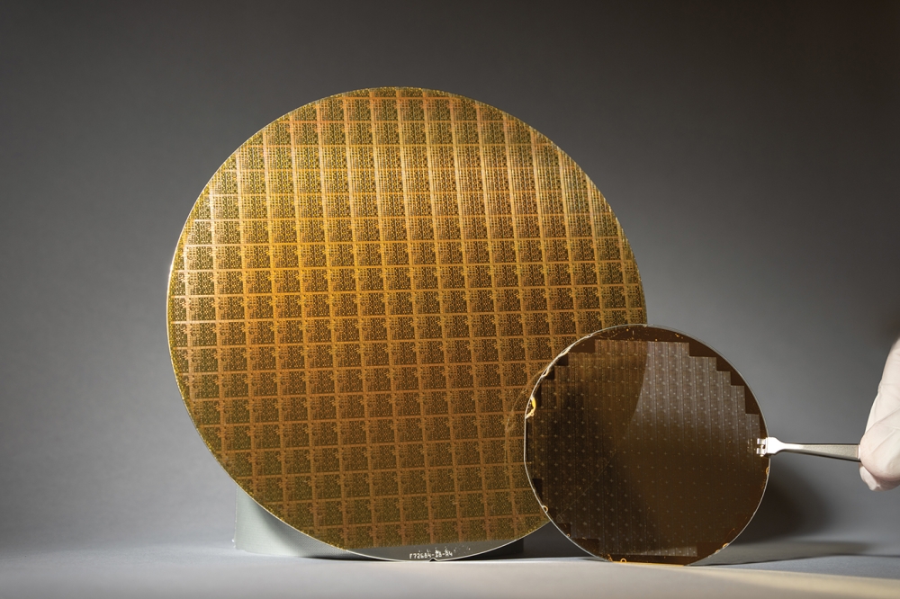
The researchers packed two processor cores with more than 70 million transistors and 850 photonic components onto a 3-by-6-millimeter chip. They fabricated the microprocessor in a foundry that mass-produces high-performance computer chips, proving that their design can be easily and quickly scaled up for commercial production.
The new chip, described in a paper to be published Dec. 24 in the print issue of the journal Nature, marks the next step in the evolution of fibre optic communication technology by integrating into a microprocessor the photonic interconnects, or inputs and outputs (I/O), needed to talk to other chips.
"This is a milestone. It's the first processor that can use light to communicate with the external world," said Vladimir Stojanovi, an associate professor of electrical engineering and computer sciences at the University of California, Berkeley, who led the development of the chip. "No other processor has the photonic I/O in the chip."
Stojanovi and fellow UC Berkeley professor Krste Asanovi teamed up with Rajeev Ram at the Massachusetts Institute of Technology and Milos Popovi at the University of Colorado, Boulder, to develop the new microprocessor.
"This is the first time we've put a system together at such scale, and have it actually do something useful, like run a program," said Asanovi, who helped develop the free and open architecture called RISC-V (reduced instruction set computer), used by the processor.
The researchers came up with a number of key innovations to harness the power of light within the chip.
Each of the key photonic I/O components - such as a ring modulator, photodetector and a vertical grating coupler - serves to control and guide the light waves on the chip, but the design had to conform to the constraints of a process originally thought to be hostile to photonic components. To enable light to move through the chip with minimal loss, for instance, the researchers used the silicon body of the transistor as a waveguide for the light. They did this by using available masks in the fabrication process to manipulate doping, the process used to form different parts of transistors.
After getting the light onto the chip, the researchers needed to find a way to control it so that it can carry bits of data. They designed a silicon ring with p-n doped junction spokes next to the silicon waveguide to enable fast and low-energy modulation of light.
Using the SiGe parts of a modern transistor to build a photodetector took advantage of germanium's ability to absorb light and convert it into electricity.
A vertical grating coupler that leverages existing poly-silicon and silicon layers in innovative ways was used to connect the chip to the external world, directing the light in the waveguide up and off the chip. The researchers integrated electronic components tightly with these photonic devices to enable stable operation in a hostile chip environment.
The authors emphasised that these adaptations all worked within the parameters of existing microprocessor manufacturing systems, and that it will not be difficult to optimise the components to further improve their chip's performance.
While advances in optical communication technology have dramatically improved data transfers between computers, bringing photonics into the computer chips themselves had been difficult. That's because no one has figured out how to integrate photonic devices into the same complex and expensive fabrication processes used to produce computer chips without changing the process itself. Doing so is key since it does not further increase the cost of the manufacturing or risk failure of the fabricated transistors.
The researchers verified the functionality of the chip with the photonic interconnects by using it to run various computer programs, requiring it to send and receive instructions and data to and from memory. They showed that the chip had a bandwidth density of 300 gigabits per second per square millimeter, about 10 to 50 times greater than packaged electrical-only microprocessors currently on the market.
The photonic I/O uses only 1.3 picojoules per bit, equivalent to consuming 1.3 watts of power to transmit a terabit of data per second. In the experiments, the data was sent to a receiver 10 meters away and back.
"The advantage with optical is that with the same amount of power, you can go a few centimeters, a few meters or a few kilometers," said study co-lead author Chen Sun, a recent UC Berkeley Ph.D. graduate from Stojanovi's lab at the Berkeley Wireless Research Center. "For high-speed electrical links, 1 meter is about the limit before you need repeaters to regenerate the electrical signal, and that quickly increases the amount of power needed. For an electrical signal to travel 1 kilometer, you'd need thousands of picojoules for each bit."
This research has already spun off two startups this year with applications in datacentres in mind. SiFive is commercialising the RISC-V processors, while Ayar Labs is focusing on photonic interconnects. Earlier this year, Ayar Labs - under its previous company name of OptiBit - was awarded the MIT Clean Energy Prize. Ayar Labs is getting further traction through the CITRIS Foundry startup incubator at UC Berkeley.
Further down the road, this research could be used in applications such as LIDAR, the light radar technology used to guide self-driving vehicles and the eyes of a robot; brain ultrasound imaging; and new environmental biosensors.


