Loading...
News Article

Consortium Integrates Laser on Silicon with Modulator

Direct wafer bonding technique combines III-V/silicon laser with Mach Zehnder modulator to achieve 25Gbps on single channel

IRT Nanoelec, an R&D consortium focused on communication technologies using micro- and nanoelectronics, has announced the co-integration of a III-V/silicon laser and silicon Mach Zehnder modulator, using direct wafer bonding. 

The team has demonstrated 25 Gbps transmission on a single channel, a rate usually achieved using an external source over a 10 km single-mode fibre.

Current interconnect technologies, which use micro-optics integration to assemble a discrete laser and a silicon photonic circuit, will soon reach their limits and new, different solutions will have to be found to handle increasing traffic, according to the researchers. Integrating photonics capabilities on silicon chips will vastly increase bandwidth, density and reliability, while dramatically reducing energy consumption. In the age of photonics-on-silicon, data transmission will be measured in terabits per second.

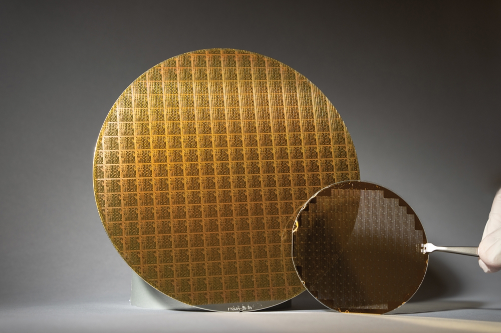
To achieve these recent results, silicon photonics circuits integrating the modulator were processed first on a 200mm SOI wafer, although 300mm wafers also could be used in the near future. Then, a two-inch wafer of III-V material was directly bonded on the wafer. In the third step, the hybrid wafer was processed using conventional semiconductor and/or MEMS process steps to produce an integrated modulator-and-laser transmitter.

"Jointly obtained by STMicroelectronics and Leti in the frame of the IRT Nanoelec cooperation, these results, especially fabricating the laser directly on silicon, demonstrate IRT Nanoelec's worldwide leadership in III/V-on-silicon integration to achieve high-data-rate fiber-optic modules," said Stéphane Bernabé, project manager. "IRT Nanoelec and its partners on this project, Leti, STMicroelectronics, Samtec and Mentor Graphics, are paving the way to integrating this technology in next-generation transceivers for optical data links."


SiC patenting strong in Q4 2024, says KnowMade
Say hello to the heterogeneous revolution
Double heterostructure HEMTs for handsets
AlixLabs to collaborate with Linköping University
SiC MOSFETs: Understanding the benefits of plasma nitridation
Wolfspeed reports Q2 results
VueReal secures $40.5m to scale MicroSolid printing
Mitsubishi joins Horizon Europe's FLAGCHIP project
Vishay launches new high voltage SiC diodes
UK team leads diamond-FET breakthrough
GaN adoption at tipping point, says Infineon
BluGlass files tuneable GaN laser patents
QD company Quantum Science expands into new facility
Innoscience files lawsuit against Infineon
Riber revenues up 5% to €41.2m
Forvia Hella to use CoolSiC for next generation charging
Photon Design to exhibit QD simulation tool
Ortel transfers CW laser fabrication to Canada
Luminus adds red and blue multi-mode Lasers
PseudolithIC raises $6M for heterogeneous chiplet tech
Mesa sidewall design improves HV DUV LEDs
IQE revenue to exceed expectations
'Game-changing' VCSEL system targets clinical imaging
German start-up secures finance for SiC processing tech
Macom signs preliminaries for CHIPS Act funding
IQE and Quintessent partner on QD lasers for AI
EU funds perovskite tandems for fuel-free space propulsion
EU to invest €3m in GeSi quantum project
Transforming the current density of AlN Schottky barrier diodes
Turbocharging the GaN MOSFET with a HfO₂ gate
Wolfspeed launches Gen 4 SiC MOSFET technology
Report predicts high growth for UK's North East
×
Search the news archive

To close this popup you can press escape or click the close icon.
Logo
x
Logo
×
Register - Step 1

You may choose to subscribe to the Compound Semiconductor Magazine, the Compound Semiconductor Newsletter, or both. You may also request additional information if required, before submitting your application.


Please subscribe me to:


You chose the industry type of "Other"

Please enter the industry that you work in: