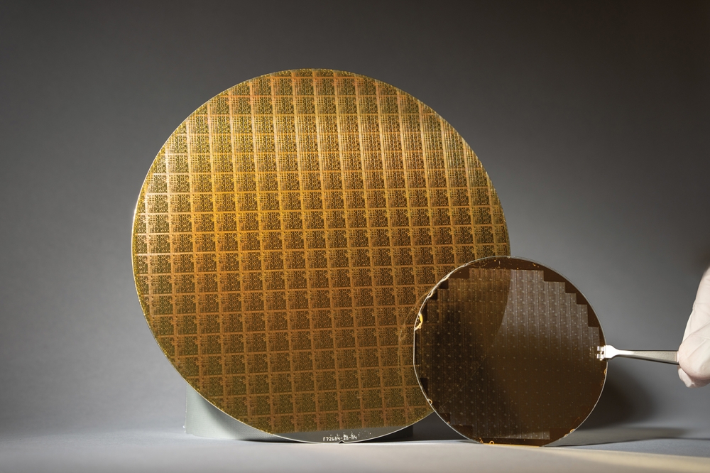
Practical silicon light at last?

A III-V quantum dot laser on silicon is set to make fast chips with built-in optics a reality. Compound Semiconductor reports.
Researchers from University College London, Cardiff and Sheffield have fabricated III-V lasers on silicon with long lifetimes.
Late last month UK-based researchers revealed the first practical, electrically-driven 1300 nm quantum dot laser grown directly on a silicon substrate, paving the way to the full integration of photonic and electronic circuits.
With an overall performance to rival III-V quantum well lasers and III-V quantum dot lasers on GaAs and SiGe, the continuous wave InAs/GaAs laser has a low threshold current, room temperature output power exceeding 105 mW and operation up to 120°C.
Crucially, with more than a mighty 3100 hours of continuous wave operating time collected, Professor Huiyun Liu from University College London (UCL) and colleagues reckon the mean time to failure of the devices will be more than 100,000 hours.
"Other photonics components have evolved and the silicon laser is the last challenge to be realised for reliable and cost-effective silicon-based photonics-electronic integration," highlights Liu. "Our demonstration opens up new possibilities for silicon photonics and the direct integration of optical interconnects on silicon microelectronics platforms."
According to Liu, the breakthrough follows six years of research, during which time he and colleagues have focused on producing high quality GaAs-on-silicon layers, via MBE, with a low defect density.
Lattice mismatch and incompatible thermal expansion coefficients between III-V materials and the silicon substrate lead to threading dislocations, which have stifled the monolithic growth of III-V lasers on silicon.
So, with this in mind, the researchers combined an AlAs nucleation layer and InGaAs/GaAs dislocation filter layers with in situ thermal annealing to minimise dislocation development.
As Liu points out, the thin AlAs nucleation layer deposited on the silicon wafer, first provided a good interface for subsequent III-V material growth. Three GaAs layers were then grown onto the nucleation layer, confining most defects to the first 200 nm region of the structure.
Super-strained dislocation filter layers were grown on top of a GaAs buffer layer which enhanced lateral motion of the threading dislocations that had formed, increasing the probability of dislocation annihilation.
MBE growth was then paused to anneal these layers, again enhancing dislocation movement and annihilation.
![]()
Scanning electron microscopy image of entire III-V laser on silicon. [Liu]
Liu reckons these processing steps reduced dislocation density to the order of 105 cm-2 - compared to ~1010 cm-2 at the GaAs/Si interface - with a standard five layer quantum dot laser then grown on top of these layers.
But for Liu, the most crucial step to achieving the laser has been to use quantum dots. As he points out, thanks to carrier localisation, quantum dots have proven to be less sensitive to threading dislocation defects than quantum well structures.
What's more, quantum dots can either pin or propel a dislocation away, with an array of quantum dots generating a strain field that prevents dislocation motion.
As the researcher says: "Any defects in the III-V layer of a quantum well device will grow over time, so while you might get a laser, you will not get the long lifetime to go with it."
"But for a quantum dot laser, dislocations in its active region may destroy a few quantum dots but the massive majority will remain active and able to provide optical gain, giving you a much longer lifetime," he adds.
And with an extrapolated lifetime of more than 100,000 hours, at least double that of quantum well lasers developed by other research groups, the scheme appears to have worked.
Silicon photonics integration
From the silicon photonics' industry perspective, the fact that Liu's III-V laser is grown directly onto a silicon substrate is the key breakthrough, opening the door to the use of silicon lasers as optical interconnects on microelectronics chips.
In the past, high performance quantum dot lasers have been successfully demonstrated on Ge-on-silicon substrates, offering an indirect route to III-V and silicon integration.
But according to Liu: "It is difficult to couple light through the germanium layer to a silicon waveguide, due to the large optical absorption coefficient of germanium at telecommunications wavelengths."
"And as well as absorbing light at telecoms wavelengths, the germanium layer restricts the range of silicon circuits to which the laser can be applied," he adds. "So a high performance III-V laser directly grown on a silicon substrate is the preferred solution for silicon photogenic-electronic integration."
So the next step for Liu and colleagues is to integrate the lasers with silicon waveguides, modulators and detectors, and finally the CMOS, a process that Liu believes will take around five years.
"There is no big stumbling block here but it will take some time and funding from industry to make it happen," says Liu. "We've always been thinking about integration, otherwise what would be the point of putting a laser on silicon?"
"It is a challenge but it's a much smaller challenge than getting the laser on silicon," he adds.


