All eyes on Allos

As Allos Semiconductors celebrates epiwafer success, CEO Bukhard Slischka claims his company can get customers ready for market faster than ever before.
In less than twelve weeks, Allos transferred its GaN-on-silicon power semiconductor epiwafer technology to an unnamed company.
Only last month, Germany-based Allos Semiconductors revealed it had transferred its GaN-on-silicon power semiconductor epiwafer technology to a 'major international industry player' in less than twelve weeks.
Remaining tight-lipped on which of its customers this is, Allos claims this move will kick-start GaN-on-silicon power semiconductor production for that company, so it can compete with industry front-runners that have already spent years and millions of dollars doing just this.
As chief executive Burkhard Slischka tells Compound Semiconductor: "Our philosophy is that our customers' engineers are very involved from day one, so after twelve weeks the process is established on their MOCVD reactor and staff possess ownership of the technology."
"At the same time, we guarantee wafer level specifications that are the best class in the world," he adds.
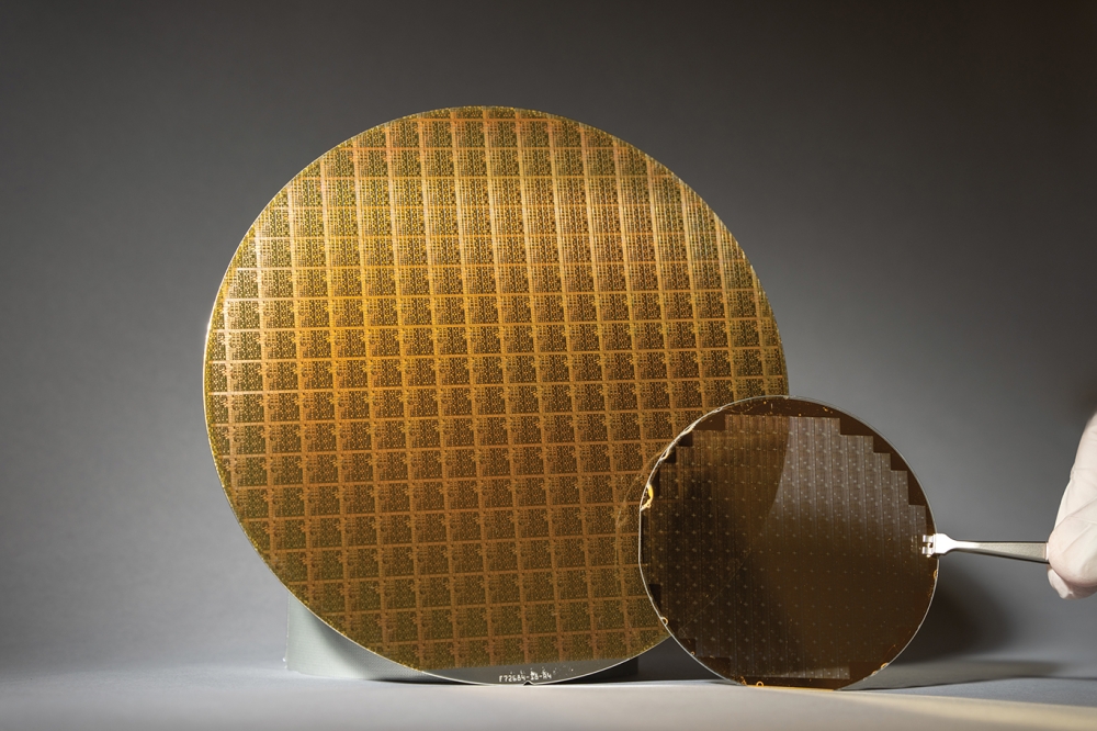
![]() After twelve weeks the Allos process can be established in a customer's MOCVD reactor
After twelve weeks the Allos process can be established in a customer's MOCVD reactor
Allos Semiconductors' history is deeply rooted in Azzurro's pioneering GaN-on-silicon developments. The Germany-based epiwafer vendor had spent more than a decade developing and selling engineered on-silicon epiwafers for LED and power electronics applications that were supplied to Osram, Epistar, and more.
Operations ceased in early 2014, but six months later, former Azzurro employees unveiled fabless Allos Semiconductors, having bought all intangible assets including the technology, IP and patents. Setting out to license its IP while transferring the technology to customers' reactors, Allos soon revealed it was working with long-time partner, Epistar.
Less than six months later, Allos' 150 mm and 200 mm processes were transferred to the Taiwan-based LED chip manufacturer. These results coincided with Epistar signing a global cross-licensing agreement with Cree, covering LED chip patents.
According to Slischka, Allos has continued to invest in research and development.
"Technology-wise we have come a long way and we now provide fundamentally improved product generation," he highlights. "Compared to results at Azzurro, we have, for example, enhanced uniformity, much better electrical performance as well as further improved crystal quality and bow control."
And while also promising good yields and fast growth times, Allos claims that the production cost per wafer area is on par with that for today's GaN-on-sapphire LED wafers.
Ready for market
As well as product quality and cost, Slischka also believes manufacturability is key. "You may be able to grow layers with a high breakdown voltage but this is worthless if you, say, have problems with wafer breakage," he says.
"Without the correct strain engineering between the GaN and silicon substrate, it is extremely difficult to get good yield. So for us, manufacturability is about balancing all the properties you need throughout the entire manufacturing process to get low cost devices," he explains.
According to the chief executive, Allos offers a process that will meet the required wafer parameters, yields and costs. "There is no point in achieving certain hero values for, say, breakdown voltage if the wafers are then prohibitively expensive," he adds.
Once licensing and technology transfer are in place, Allos can also offer what it calls 'development of customised solutions'. In it latest project, Allos will continue to work with its current, unnamed customer to get devices ready for market.
"Companies such as International Rectifier and Transphorm started developing GaN-on-silicon many years ago and have products in the market," he says. "We can help a company, which is not necessarily within the top tier group of its industry, to catch up quickly and have world-class results."
And as the chief executive highlights, these companies need to act fast.
"You really need to have fast device feedback cycles as this is typically a bottle-neck. During development, we can complete several epi-development runs a day and work on the epiwafer performance each time," he says. "To fully assess the impact on device performance, a company may need to wait months for the device processing and characterisation to be completed. But with the right set-up, customers can cut this feedback cycle time to less than two weeks."
"This is the deal for the customer in the end," he concludes. "You could probably do this yourself but why would you when by working with us you get results much faster, at a much lower cost and with a lot less risk."


