Compound Photonics shows off tiny laser-based imaging device

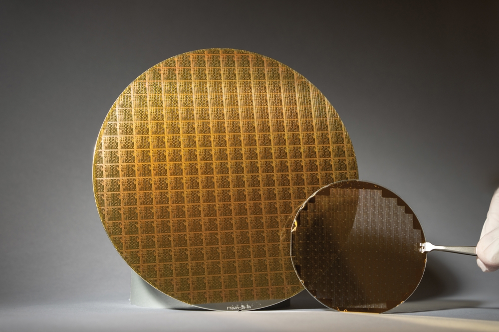
Compound Photonics, an eight-year old technology company with primary manufacturing sites in the UK and USA, has released what it claims is the world's smallest native 4K imaging device. Measuring only 14mm diagonally and featuring pixels smaller than three microns, the device is based on the company's red, green and blue semiconductor lasers.
"Compound Photonics is the biggest and most capable photonics and projector manufacturer that you have most likely never heard of," declared Tim Anderson, the company's VP of product management in his presentation at the Display Summit China 2016 held in Yixing this week.
"We are the company that has succeeded in introducing the world to RGB solid state laser based technology, making it finally possible to manufacture a 3,000 lumen lamp-less native 4K projector that rivals the performance delivered by today's solid state displays."
According to Anderson, the use of RGB laser technology eliminates lamps, creates a huge new colour gamut to work with, and enables balancing the colour output of each colour channel to achieve a perfect white point. What's more, Anderson asserted, Compound Photonics has invested significant engineering resources to reduce the cost of RGB lasers and speckle.
"Projector customers around the world want to be able to project a huge image in full daylight and still have an outstanding image," Anderson said. "Our engineers have developed specific algorithms that use an expanded colour gamut made possible by RGB laser technology. These algorithms combat ambient light and dramatically improve color contrast."
Anderson said that Compound Photonics offered capabilities ranging from tiny, bright, full HD laser light engines for mobile devices, an embedded 1080P projector that is less than two cubic centimeters in size, IR and Green lasers, head-up car displays, near-eye augmented reality, and gesture recognition.
The company owns a GaAs wafer fab in Newton Aycliffe, UK and it also has a semiconductor processing facility in Phoenix, Arizona where it manufactures liquid crystal on silicon displays and optics systems for its laser projection light engines
"We are a team of over 300 scientists, technologists, software engineers, and marketers that are committed to changing the way consumers interact with technology. Our corporate directory is a veritable 'who's who' of technology and includes veterans of IBM, InFocus, Epson, NEC, Philips, Pixelworks and Microsoft," he said.


