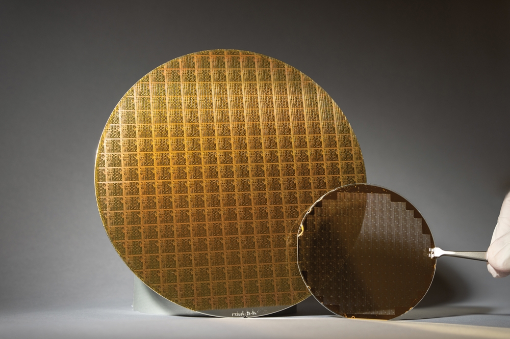
ClassOne Announces Gold Plating savings

ClassOne Technology is reporting significant savings in the plating of gold for 200mm or smaller wafers using its Solstice electroplating tools.
Solstice systems are designed for smaller-substrate users in technologies such as MEMs, LEDs, power devices, RF communications, interposers, photonics and microfluidics.
The savings come from elimination of gold waste, faster and simpler processing, and innovative Solstice-enabled techniques that can substantially reduce gold usage, says the company.
"Many users have been spending millions of dollars on gold each year," said Byron Exarcos, president of ClassOne Group. "It's a major issue, especially in emerging markets such as lasers, LEDs, RF and MEMS which often require gold layers as thick as 3 to 35 microns. "That's why they're becoming keenly interested in Solstice to cut their gold spending."
Kevin Witt, president of ClassOne Technology said: "Previously used CVD and PVD methods deposited gold not just on the wafer but also on the entire chamber interior. That 'oversprayed' gold was difficult to remove and inefficient to reclaim - which led to a considerable net loss of gold. By contrast, Solstice deposits only on the wafer, so there's no gold waste, and no need for cleaning or gold reclamation efforts."
Witt pointed out that Solstice economies also come from its higher gold deposition speed. Plating at 150 to 300nm/min, it is roughly ten times faster than CVD and PVD methods. In addition, Solstice starts processing immediately, not requiring an hour or more for pump-down as vacuum-based tools do. All of this translates to additional savings, from higher throughput and more cost-efficient production.
The eight-chamber design of the Solstice S8 enables it to replace a solid gold layer with a multi-metal stack - and reduce gold usage substantially. For example, a feature that previously required a 5µm layer of solid gold can now be replaced with a "˜sandwich' of 0.25µm Au, 1µm Ni, 2.5µm Cu, another 1µm Ni, topped with 0.25µm Au - to achieve equivalent functionality while reducing gold usage by a factor of ten.
And Solstice's multi-chamber design enables it to deposit all five layers in a single cycle; so no additional process steps or time are required to gain very significant cost savings.
ClassOne noted that over a year, total gold savings can grow quite large. For example, in the case cited above, if the solid gold 5µm layer covers 50 percent of a 150mm wafer area, and if the fab is running 1500 wafers per week through a metal lift-off process and gold costs $1200 per troy ounce - even if all oversprayed gold were recovered, the user's annual gold expenditure would be roughly $2,150,000.
However, if the special Solstice multi-metal layering technique were used, the total metal cost (for Au, Ni and Cu combined) would be reduced to approximately $108,000. This would yield an annual savings of over $2,042,000, which would more than pay back the cost of a Solstice.


