
US/Hong Kong team integrates quantum dot lasers on silicon
A group of scientists from Hong Kong University of Science and Technology; the University of California, Santa Barbara; Sandia National Laboratories and Harvard University have built tiny lasers directly on silicon.
As the group reports in Applied Physics Letters, integrating subwavelength cavities - the essential building blocks of their tiny lasers - onto silicon enabled them to create and demonstrate high-density on-chip light-emitting elements.
To do this, they first had to resolve silicon crystal lattice defects to a point where the cavities were essentially equivalent to those grown on lattice-matched GaAs substrates. Nano-patterns created on silicon to confine the defects made the GaAs-on-silicon template nearly defect free and quantum confinement of electrons within quantum dots grown on this template made lasing possible.
The group was then able to use optical pumping (using light, rather than electrical current to  pump electrons from a lower energy level in an atom or molecule to a higher level) to show that the devices work as lasers.
Traditionally, the lasers used for commercial applications are quite large - typically 1 mm x 1 mm. Smaller lasers tend to suffer from large mirror loss.
But the scientists were able to overcome this issue with "tiny whispering gallery mode lasers - only 1 micron in diameter - that are 1,000 times shorter in length, and 1 million times smaller in area than those currently used," said Kei May Lau, at the department of electronic and computer engineering, Hong Kong University of Science and Technology.
Whispering gallery mode lasers are considered an extremely attractive light source for on-chip optical communications, data processing and chemical sensing applications.
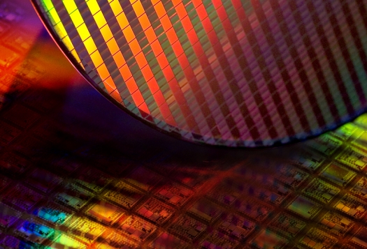
"Our lasers have very low threshold and match the sizes needed to integrate them onto a microprocessor," Lau pointed out. "And these tiny high-performance lasers can be grown directly on silicon wafers, which is what most integrated circuits (semiconductor chips) are fabricated with."
In terms of applications, the group's tiny lasers on silicon are suited for high-speed data communications.Â
"Photonics is the most energy-efficient and cost-effective method to transmit large volumes of data over long distances. Until now, laser light sources for such applications were 'off chip' - missing - from the component," Lau explained. "Our work enables on-chip integration of lasers, an [indispensable] component, with other silicon photonics and microprocessors."
The researchers expect to see this technology emerge in the market within ten years.
Next, the group is "working on electrically pumped lasers using standard microelectronics technology," Lau said.
'Sub-wavelength InAs quantum dot micro-disk lasers epitaxially grown on exact Si (001) substrates' by Yating Wan et al: Applied Physics Letters May 31, 2016Â


