Loading...
News Article

CoorsTek Unveils GaN-on-Silicon wafers at ISPSD 2016

News
Semiconductor ceramics company supports power electronics fabrication with epiwafers, ceramic substrates, and custom processing components


CoorsTek, a supplier of engineered ceramics, will unveil its enhanced GaN-on-silicon epiwafers at next week's International Symposium on Power Semiconductor Devices and ICs (ISPSD) in Prague, Czech Republic.

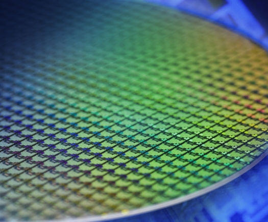
CoorsTek will be displaying the combined capabilities of CoorsTek and Covalent Materials (formerly Toshiba Ceramics, now CoorsTek KK) including: GaN-on-Si Epiwafers for power devices and integrated circuits; AlN substrates for hybrid circuits; and engineered ceramic components for semiconductor processing equipment made from PureSiC CVD SiC, PlasmaPure High-Purity alumina, and other technical ceramics.

"The latest CoorsTek GaN-on-silicon technology helps customers achieve higher device manufacturing yields and breakdown voltages based on lower defect densities and leakage current," explains Jun Komiyama, R&D manager at CoorsTek. "The shift from 150mm to 200mm diameter GaN-on-Si process is also improving the economics for power electronics in electric and hybrid automobiles, solar photovoltaic inverters, RF and microwave power, and more."

On June 1, CoorsTek announced its acquisition of the Philips ceramic operation in Uden, Netherlands  - extending its footprint to a dozen European manufacturing locations in the Czech Republic, England, Finland, Germany, Italy, Netherlands, Norway, Scotland, and Sweden.

Say hello to the heterogeneous revolution
Double heterostructure HEMTs for handsets
AlixLabs to collaborate with Linköping University
SiC MOSFETs: Understanding the benefits of plasma nitridation
Wolfspeed reports Q2 results
VueReal secures $40.5m to scale MicroSolid printing
Mitsubishi joins Horizon Europe's FLAGCHIP project
Vishay launches new high voltage SiC diodes
UK team leads diamond-FET breakthrough
GaN adoption at tipping point, says Infineon
BluGlass files tuneable GaN laser patents
QD company Quantum Science expands into new facility
Innoscience files lawsuit against Infineon
Riber revenues up 5% to €41.2m
Forvia Hella to use CoolSiC for next generation charging
Photon Design to exhibit QD simulation tool
Ortel transfers CW laser fabrication to Canada
Luminus adds red and blue multi-mode Lasers
PseudolithIC raises $6M for heterogeneous chiplet tech
Mesa sidewall design improves HV DUV LEDs
IQE revenue to exceed expectations
'Game-changing' VCSEL system targets clinical imaging
German start-up secures finance for SiC processing tech
Macom signs preliminaries for CHIPS Act funding
IQE and Quintessent partner on QD lasers for AI
EU funds perovskite tandems for fuel-free space propulsion
EU to invest €3m in GeSi quantum project
Transforming the current density of AlN Schottky barrier diodes
Turbocharging the GaN MOSFET with a HfO₂ gate
Wolfspeed launches Gen 4 SiC MOSFET technology
Report predicts high growth for UK's North East
Element Six unveils Cu-diamond composite
×
Search the news archive

To close this popup you can press escape or click the close icon.
Logo
x
Logo
×
Register - Step 1

You may choose to subscribe to the Compound Semiconductor Magazine, the Compound Semiconductor Newsletter, or both. You may also request additional information if required, before submitting your application.


Please subscribe me to:


You chose the industry type of "Other"

Please enter the industry that you work in: