ADVA joins EU Lasers-on-Silicon consortium

ADVA Optical Networking has announced that it is playing a key role in the EU-funded Directly Modulated Lasers on Silicon (DIMENSION) project. DIMENSION, which brings together a consortium of research and industry partners from four European countries, aims to create a platform for single-chip electro-optical integration.
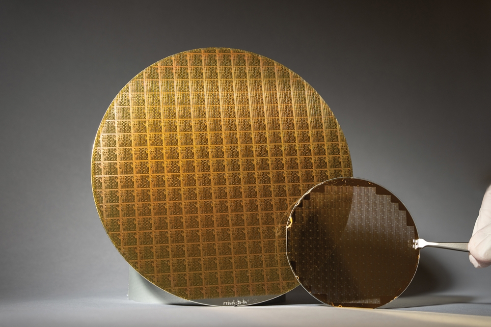
The breakthrough technology it produces will involve lasers built with active III-V materials embedded into silicon photonics chips. This will generate the versatile, cost-efficient components needed to optimise datacentre interconnect (DCI) transport and create the next generation of datacentre.
The four-year project ( funded by the European Union's Horizon 2020 research and innovation program) aims to take electro-optical integration to a new level by producing silicon chips built with active laser components. The consortium of partners also forms a complete value chain for the production of the new technology, from research through to innovative package design and assembly. The project will run until the end of January 2020..
"DIMENSION unites specialists from different fields and enables us to address the complete value chain of directly modulated lasers, from materials research to application," said Bert Offrein, manager, photonics, IBM Research - Zurich. "What we're bringing to the table is a lot of experience with transformational datacentre innovation. We're focusing on incorporating highly efficient III-V materials into silicon chips. Our role is to design and produce the integrated active optical components.
"This technology will bring the optics to where the data is generated and that leads to improvements in every part of the datacentre. By enhancing interconnections at different reaches, from centimetres up to kilometres, we'll be able to reduce size, cost and power on links between boards, computers and facilities."
The DIMENSION project is coordinated by Dresden University of Technology and involves partners from Germany, Switzerland, Greece and the UK. The two research centres included are Innovations for High Performance Microelectronics and Athens Information Technology. The large industry partners are ADVA Optical Networking, Optocap and IBM Research - Zurich.
"Improving efficiency in the DCI couldn't be more vital given the increasing demand for cloud computing and the growing scale of the internet of things," commented Michael Eiselt, director, advanced technology, ADVA Optical Networking.
"Much of our recent innovation has centered on enhancing the DCI, such as our FSP 3000 CloudConnect solution. By integrating the three distinct technologies of silicon photonics, electronics and active photonics, we're giving data centers what they need to meet tomorrow's demands. It's great to be working closely with other European companies and institutions to make this vital breakthrough a reality. It also provides fantastic opportunities for university students who get to be at the forefront of innovation and help make a significant impact on the industry."


