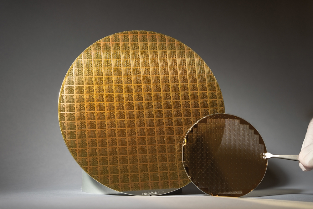
UK funding competition: compound semiconductor applications
Innovate UK is to invest up to £4 million in innovative projects that help to speed up the use of compound semiconductors. This is in areas such as power electronics, RF/microwave, photonics and sensors. The competition opens: Monday 18 July 2016, and applications close noon on Wednesday 26 October 2016.
The organisers are seeking proposals with large and scalable commercial potential. The aim of this competition is to ensure that UK businesses can respond to market opportunities in compound semiconductors.
Compound semiconductors offer improved performance for applications that currently use silicon-based semiconductors. They open up new application areas that silicon-based semiconductors cannot. But there are technical and business risks across the supply chain. So the development and adoption of new compound semiconductor devices is often held back.
This competition aims to address some of the technical challenges. This is so that businesses can exploit the superior performance of compound semiconductors.
Projects must involve a compound semiconductor material with a scalable market application. Examples of compound semiconductors include: GaAs, GaN, InP, SiC and HgCdTe (gallium arsenide, gallium nitride, indium phosphide, silicon carbide and mercury cadmium telluride).
Organisers are particularly interested in projects that address one or more of the following:
- thermal management technologies for compound semiconductor packaging, such as multi-phase fluidics
- materials and techniques that enable a significant improvement in device performance. Examples include operating speed, temperature, voltage, current, or light intensity
- rapid prototyping techniques, such as additive manufacturing using polymers or ceramics, for advanced packaging or printed die interconnects
- simulation and modelling techniques, such as multi-scale or multi-physics at device or sub-system level, to speed up verification and validation, and reduce development cycles
- novel adhesion technologies to join dissimilar materials, such as graphene-loaded epoxy
- approaches to combine multi-mode devices. Examples include integrating photonic with RF devices or photonic with high-voltage devices
- approaches to create hybrid combinations of silicon die with compound semiconductor die
- techniques to enable rapid alignment and assembly. These will help to automate more of the supply chain and improve productivity
- automated or semi-automated test methodologies for power electronic, RF/microwave, photonics or sensor applications
- projects that lead to a significant reduction in cost across the supply chain


