Loading...
News Article

HexaTech Demos High Performance UV-C LED

News
First generation AlN-based device achieves 6mW in 0.15mm2 active area

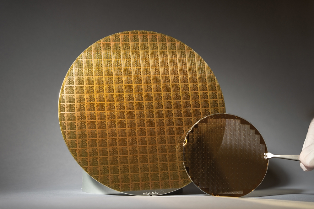
HexaTech has demonstrated its first generation UVSure UV-C LED, based on the company's proprietary AlN substrate material.

The 263nm wavelength device achieves 6mW in a 0.15mm2 active area die. When scaled to its second generation larger footprint, the die is expected to produce approximately 24mW, which is twice the radiant flux of competitive products.

Further, when driven in pulse mode to 300mA, the same 0.15mm2 active area die is able to reach 19mW, or approximately 76mW in the large die format.

"This demonstration is a milestone in our business, and is the direct result of intense device R&D coupled with the use of our exclusive high quality AlN substrate material," stated HexaTech CEO John Goehrke.

He added, "This capability allows us to engage the UV-C LED market at the right moment, linking together incredibly strong interest with cutting-edge performance. It also clearly demonstrates our continued assertion that the best substrate material yields the best device performance, and this first generation result is just the beginning."

"We are truly excited to be in a position to support the rapidly expanding UV-C LED customer interest seen over the last several years," remarked Gregory Mills, HexaTech's director of business development. "With point-of-use (POU) sterilization applications alone representing a $400M plus opportunity in the coming years, we anticipate significant corporate expansion and strategic customer engagement," he noted.

Joseph Smart, director of LED development commented: "HexaTech's world-leading, high quality bulk AlN substrates are the essential foundation for attaining these results, enabling near perfect epitaxial growth quality throughout the active region of the device, essential to produce both high internal quantum efficiency (IQE) and long component lifetimes. This is something that competing sapphire substrate technology simply cannot sustain at these wavelengths."

Say hello to the heterogeneous revolution
Double heterostructure HEMTs for handsets
AlixLabs to collaborate with Linköping University
SiC MOSFETs: Understanding the benefits of plasma nitridation
Wolfspeed reports Q2 results
VueReal secures $40.5m to scale MicroSolid printing
Mitsubishi joins Horizon Europe's FLAGCHIP project
Vishay launches new high voltage SiC diodes
UK team leads diamond-FET breakthrough
GaN adoption at tipping point, says Infineon
BluGlass files tuneable GaN laser patents
QD company Quantum Science expands into new facility
Innoscience files lawsuit against Infineon
Riber revenues up 5% to €41.2m
Forvia Hella to use CoolSiC for next generation charging
Photon Design to exhibit QD simulation tool
Ortel transfers CW laser fabrication to Canada
Luminus adds red and blue multi-mode Lasers
PseudolithIC raises $6M for heterogeneous chiplet tech
Mesa sidewall design improves HV DUV LEDs
IQE revenue to exceed expectations
'Game-changing' VCSEL system targets clinical imaging
German start-up secures finance for SiC processing tech
Macom signs preliminaries for CHIPS Act funding
IQE and Quintessent partner on QD lasers for AI
EU funds perovskite tandems for fuel-free space propulsion
EU to invest €3m in GeSi quantum project
Transforming the current density of AlN Schottky barrier diodes
Turbocharging the GaN MOSFET with a HfO₂ gate
Wolfspeed launches Gen 4 SiC MOSFET technology
Report predicts high growth for UK's North East
Element Six unveils Cu-diamond composite
×
Search the news archive

To close this popup you can press escape or click the close icon.
Logo
x
Logo
×
Register - Step 1

You may choose to subscribe to the Compound Semiconductor Magazine, the Compound Semiconductor Newsletter, or both. You may also request additional information if required, before submitting your application.


Please subscribe me to:


You chose the industry type of "Other"

Please enter the industry that you work in: