Metrology: making the most of market growth

As III-V markets gather momentum, LayTec is chasing the opportunities, reports Compound Semiconductor.
LayTec is intent on winning business as III-V markets grow.
In late June, this year, Berlin-based instrumentation supplier, LayTec, announced its first order for in-situ metrology tool, EpiTT/VCSEL.
Designed for VCSEL applications, the tool measures wafer temperature and growth rate of epitaxy layers during MOCVD, but also monitors the spectral reflectance of the evolving distributed Bragg reflector and cavity structures.
As chief technology officer, Kolja Haberland, highlights: "We look at the spectroscopic position of the stop-band and see if there is any mis-matching between the cavity and Bragg reflectors."
"Mirrors, for example, have to reflect at the same wavelength and even with a mismatch of only a couple of nanometres, device performance will suffer," he adds. "We are trying to bring new tools into the market that serve customer needs, and we see great growth potential in the VCSEL market."
The company's first in-situ product, so-called EpiRAS, monitored epitaxial growth of cubic semiconductors.
Primarily a research tool, the system is still used by many academic organisations to provide data on wafer temperature, growth rate, composition, doping levels and more. But while it has infiltrated myriad research organisations, the leap to industry didn't quite happen.
"This is a very valuable tool and measures so many parameters on the wafer surface but it has been just too complex," says Haberland. "Also it only works with cubic materials such as arsenides and phosphides, so for example, we can't access the nitride market with this tool."
Given this, the last few years have been a hive of activity for LayTec, with the company developing tools, largely for use with Aixtron reactors, to take advantage of growing III-V markets.
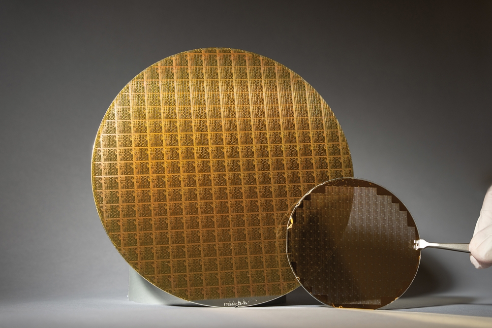
![]() As III-V markets grow, LayTec is delivering more in-situ metrology tools. [LayTec]
As III-V markets grow, LayTec is delivering more in-situ metrology tools. [LayTec]
For example, EpiTT described as the 'workhorse of mass production', has predominantly targeted industry production of GaAs and InP laser diodes, edge emitting lasers and VCSELs.
The tool measures temperature and reflectance at three wavelengths and can be supplemented with 'EpiCurve' to detect wafer bow.
Meanwhile, the company, also keen to glean business from GaN LED and laser diode markets developed 'Pyro400' to measure surface temperature during the epitaxial growth of GaN on sapphire or SiC.
As Haberland highlights, such tools have proven crucial to manufacturers in these markets as well as developers of InP and GaAs RF devices, but in October 2015, LayTec upped its game by introducing a new generation of these tools.
Described as being more customisable, crucially, the latest 'Gen3' tools can be used beyond Aixtron reactors.
"These stand alone products fit into virtually any brand of MOCVD system," says Haberland. "So we're not just talking about the Aixtron R6 and Aixtron Planetary, these can also be used with the Veeco K 700 and Taiyo Nippon Sanso UR 25K, in smaller research systems or retrofits from, say, SMI and Agnitron, as well as in a variety of plasma based etching and deposition systems."
The move follows the integration of LayTec's OEM metrology tools to Aixtron's systems just over a year ago. Then, in June this year, Aixtron qualified LayTec's Gen 3 software so users can also access the latest metrology tools on its MOCVD platform.
But be it integrated or standalone, the growing demand for in-situ metrology is all good news for LayTec, and as Haberland says: "These developments are bringing us deeper into more markets."
Market developments
Clearly LayTec is intent on capturing business as III-V markets grow. The recent delivery of the VCSEL-specific metrology tool follows customer demand to monitor progress of VCSEL growth during the many hours of deposition of the III-V materials.
As Haberland says: "If in-situ data indicates that growth isn't on track, the user can implement a control loop to bring growth back on track and optimise yield and throughput."
And as VCSEL markets grow, LayTec has also spotted a second market to focus efforts on; the UV-LED market.
"Again we see good growth here," says Haberland. "UV-LEDs are grown on different materials, AlN, AlN buffers or AlGaN buffers with a high aluminium content, so straightforward temperature measurement will not work. We are bringing a specialised version of tool, as we did with the EpiTT VCSEL, for UV-LEDs to the market."
Looking to the future, LayTec is expecting growing demand from Taiwan and China as, for example, LED manufacturers turn to the latest generation of Pyro400 to monitor epitaxy growth.
Global LED players have already adopted the tool but according to Haberland: "[Asia-based manufacturers] are catching up and will integrate these tools to their control loops to bring more value to mass production."
The company also recently revealed that epiwafer manufacturer, IQE, has equipped its fab with LayTec Gen3 metrology systems for MOCVD process monitoring.
The move is just one of several partnerships that LayTec has forged with foundries, which Haberland sees as all being crucial to the company's future.
"These foundries run on many tools and have a huge variety of growth processes for different customers, products wafer sizes and materials," he says. "Calibration is so important here, so in situ metrology makes sense."
Still, for LayTec, there is much more beyond MOCVD. "Our market studies look at the number of MOCVD tools sold in different markets and there is a lot of growth predicted for UV LEDs, GaN on silicon power devices, with GaAs and InP markets remaining steady," says Haberland.
"But we see ourselves also reaching broader markets, and these will include plasma-enhanced CVD, ALD and MBE of lots of materials from pure silicon and SiGe to III-V on silicon and CMOS integration." he adds.


