US team develops hexagonal BN nuclear detectors

To prevent terrorists from smuggling nuclear weapons into its ports, the US Security and Accountability for Every Port Act mandates that all overseas cargo containers be scanned for possible nuclear materials or weapons.
This is done by detecting neutron signals with detectors based on scarce and costly Helium-3 gas. Now a group of Texas Tech University researchers has developed an alternative approach based on hexagonal BN semiconductors.
The team, led by Hongxing Jiang and Jingyu Lin, think the material fulfills many key requirements for helium gas detector replacements and can serve as a low-cost alternative in the future.
The group's concept was first proposed to the US Department of Homeland Security's Domestic Nuclear Detection Office and received funding from its Academic Research Initiative program six years ago. It has just reported its results in the journal Applied Physics Letters.
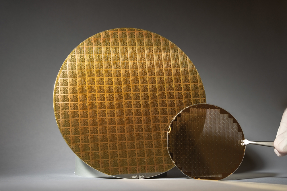
By using a 43-micron-thick hexagonal boron-10 enriched nitride layer, the group created a thermal neutron detector with 51.4 percent detection efficiency, which is a record high for semiconductor thermal neutron detectors.
"Higher detection efficiency is anticipated by further increasing the material thickness and improving materials quality," explained Jiang, Nanophotonics Center and Electrical & Computer Engineering, Whitacre College of Engineering, Texas Tech University.
"Our approach of using hexagonal BN semiconductors for neutron detection centers on the fact that its boron-10 isotope has a very large interaction probability with thermal neutrons," Jiang continued. "This makes it possible to create high-efficiency neutron detectors with relatively thin hexagonal BN layers. And the very large energy bandgap of this semiconductor - 6.5 eV - gives these detectors inherently low leakage current densities."
The key significance of the group's work? This is a completely new material and technology that offers many advantages.
"Compared to helium gas detectors, boron nitride technology improves the performance of neutron detectors in terms of efficiency, sensitivity, ruggedness, versatile form factor, compactness, lightweight, no pressurisation ... and it's inexpensive," Jiang said.
This means that the material has the potential to revolutionize neutron detector technologies.
"Beyond special nuclear materials and weapons detection, solid-state neutron detectors also have medical, health, military, environment, and industrial applications," he added. "The material also has applications in deep ultraviolet photonics and two-dimensional heterostructures. With the successful demonstration of high-efficiency neutron detectors, we expect it to perform well for other future applications."
The main innovation behind this new type of neutron detector was developing hexagonal BN with epitaxial layers of sufficient thickness - which previously didn't exist.
"It took our group six years to find ways to produce this new material with a sufficient thickness and crystalline quality for neutron detection," Jiang noted.
Based on their experience working with III-nitride wide bandgap semiconductors, the group knew at the outset that producing a material with high crystalline quality would be difficult.
"It's surprising to us that the detector performs so well, despite the fact that there's still a little room for improvement in terms of material quality," he said.
One of the most important impacts of the group's work is that "this new material and its potential should begin to be recognized by the semiconductor materials and radiation detection communities," Jiang added.
Now that the group has solved the problem of producing hexagonal BN with sufficient thickness, as well as crystalline quality to enable the demonstration of neutron detectors with high efficiency, the next step is to demonstrate high-sensitivity of large-size detectors.
"These devices must be capable of detecting nuclear weapons from distances tens of meters away, which requires large-size detectors," Jiang added. "There are technical challenges to overcome, but we're working toward this goal."
'Realization of highly efficient hexagonal boron nitride neutron detectors' by A. Maity, T.C. Doan, J. Li, J.Y. Lin and H.X. Jiang; Appl. Phys. Lett. 109, 072101 (2016)


