
Technical Insight
Perfecting 200 mM processing tools
As the demand for MEMS, sensors and mobility expands, heterogeneous devices on 200 mm substrates will become more common to address that increased demand.
Devices such as GaN-on-Si for RF (Radio Frequency)and power, and BAW/FBAR and MEMS on various substrates, will require a new generation of 200 mm process tools to satisfy the needs for high-throughput and high yield lift-off compatibility. Batch sizes will also be enlarged to match that of other process steps. High collection efficiency of precious metals will continue to a driver for reduced device cost and excellent wafer and batch film uniformity will continue to be required for new device performance across all materials of interest.
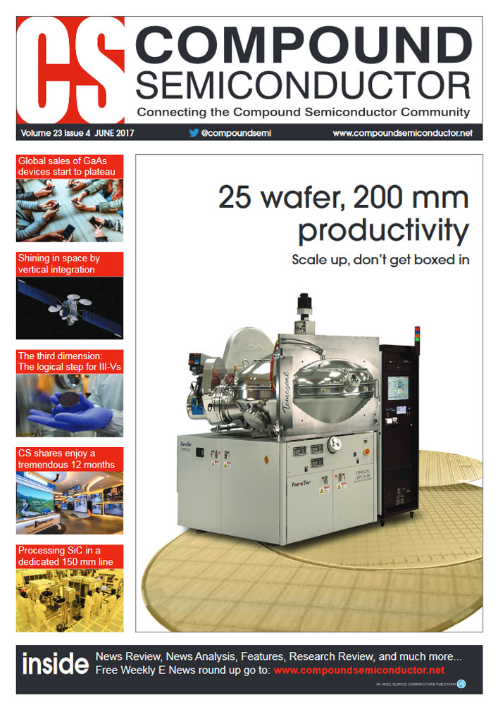
Ferrotec announces a new lift-off metal deposition system to meet these needs for 200 mm substrates, the Temescal
UEFC-6100 ultra-efficient electron beam evaporator.
A key factor to achieve high yield lift-off is the near normal incidence of the deposition across the entire wafer surface. This is best achieved with the line of sight material travel of e-beam deposition at long source-to"“substrate distances. The UEFC-6100 is designed for source-to-substrate (SR) distances of 43" (1092 mm) or 46" (1168 mm) to achieve < 5 degree incident angles at all locations on a wafer's surface.
Dual-axis and patented no-contact, magnetically driven HULA (high uniformity lift-off assembly) wafer motion ensures excellent uniformity across multiple process conditions. HULA motion also delivers the highest material collection efficiency for precious metals by minimizing the need for large area uniformity masks while maintaining a high wafer packing fraction. Throughputs are further aided by the intelligent conic chamber designs; which minimize and optimize both volume and total non-substrate coated surface areas within these systems.
These factors improve pump down times by minimizing outgassing surfaces and their coating based degradation in pump times due to condensate build-up over multiple operating cycles.
A large 25x (200 mm) wafer batch also improves throughput while limiting the need for tracking split lots that may be required in smaller tools. As the size and value of the wafers increases, automated wafer handling becomes more preferred. This new system design is matched with the Ferrotec Wafer Valet automatic wafer handling system to eliminate the need for operators to handle individual wafers, which speeds tool load and unload times and reduces the risk of handling errors.
The combined effect of all these design factors is pointed out in the table below. The table compares performance for deposition of a 1 micron thick gold layer of the UEFC-6100, with two other tool designs; an existing tool originally designed for 150 mm wafers at 43" throw distance that could hold up to 18 x 200 mm wafers, and a theoretical "best design" for a traditional box style system with a single axis of rotation carrier that could handle 25 x 200 mm wafers.
With the assumption that masking to achieve uniform films is required, it is clear the UEFC-6100 outperforms the traditional designs in all areas listed.

Table 1. Performance comparison for deposition of 1 micron gold layer


